CAN Bus Transceivers Operate from 3.3V or 5V and Withstand ±60V Faults
The LTC2875 is a robust CAN bus transceiver that features ±60V overvoltage and ±25kV ESD tolerance to reduce failures caused by electrical overstress. These transceivers introduce several new capabilities for high voltage tolerant CAN bus transceivers: operation from 3.3V or 5V supply voltages, up to 4Mbps data rate, ±36V common mode voltage range, continuously variable slew rate and availability in 3mm × 3mm DFN packages.
The CAN bus forms the backbone of many automotive, commercial and industrial data communications systems. CAN bus networks are used in a wide variety of applications, including automotive and transportation electronics, industrial control systems, supervisory control and data acquisition systems, building automation and security, HVAC control, and other custom networked systems. Robustness to electrical overstress is an important attribute for CAN bus transceivers used in these applications, which risk exposure to wiring faults, ground voltage faults and lightning induced surge voltages.
However, few CAN transceivers capable of operating from 3.3V supplies are available, and until now, none offer the high voltage tolerance and wide common mode operating range of the LTC2875. Many customers have requested a robust CAN bus transceiver with the performance and the expanded capabilities demanded by contemporary network applications. The LTC2875 transceiver is Linear Technology’s response to these requests.
3.3V Or 5V Operation
Most high voltage tolerant CAN bus transceivers can operate only from a 5V supply, but 5V is rarely used by most modern digital circuits. The CAN bus transceiver may be the only 5V component in the system. A high voltage tolerant CAN bus transceiver that operates from a 3.3V supply reduces design time and cost by eliminating the need for a dedicated 5V supply.
The LTC2875 maintains compatibility with the ISO 11898-2 CAN bus standards when operating from a 3.3V supply, driving the full specified differential bus voltage VOD and maintaining the same receiver input threshold voltages. The only difference between 3.3V and 5V operation is that the common mode bus voltage is reduced to 1.95V while operating at 3.3V, which falls below the range of 2V to 3V specified by ISO 11898-2. This minor shift in common mode voltage falls within the minimum common mode voltage range of −2V to 7V specified in the standard (and is truly inconsequential to the ±25V common mode voltage range of the LTC2875 when operating at 3.3V), allowing the LTC2875 o communicate seamlessly with any other ISO11898-2 compliant transceivers. The LTC2875 is fully interoperable with other transceivers on the same bus that are powered by 5V when operating from either a 3.3V or 5V supply.
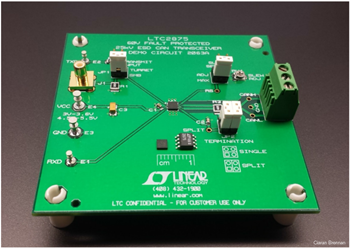
Figure 1. LTC2875 demo circuit with DFN and SO packages in foreground
4 Mbps Data Rate With High Symmetry Driver And Continuous Slew Rate Control
Modern CAN bus systems may operate at data rates that exceed the capabilities of existing high voltage tolerant transceivers. For example,Linear Technology’s LT1796 CAN transceiver operates at a maximum of 125kbps. The LTC2875 offers similar high voltage tolerance to this predecessor, but can communicate 32 times faster, up to 4Mbps.
Not all systems require a high data rate. In applications where lower data rates suffice, the system designer may prefer a CAN bus driver with low electromagnetic emissions (EME) slew controlled transitions. The LTC2875 provides a continuously variable slew rate over an approximate 20-to-1 range. The lowest slew rate is appropriate for data rates of 200kbps or less. The slew rate is programmed by a single resistor in series with the chip enable pin RS, as plotted in Figure 2.
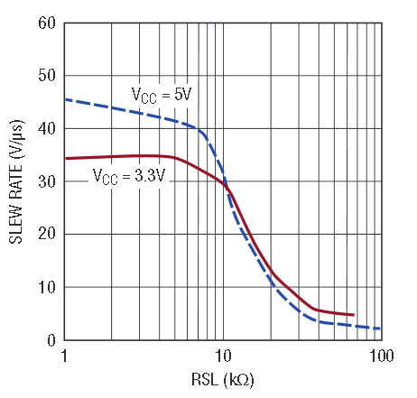
Figure 2. Slew rate vs slew control resistor RSL
Considerable design effort was made to keep the switching symmetry of the CAN transmitter highly symmetrical (or more accurately, anti-symmetrical) between the CANH and CANL outputs, because any asymmetry between the switching waveforms of the two outputs produces a change in the common mode voltage. While the electromagnetic fields produced by the differential voltage along a twisted pair largely cancel and produce little EME, the electromagnetic fields of the common mode voltage on the pair add together and may produce significant EME, particularly if the twisted pair is unshielded. Therefore, good CAN transmitter switching symmetry results in lower EME.
The LTC2875 provides two features to reduce the EME produced by fluctuations of the common mode voltage during switching: variable slew rate control and split termination. The transmitter slew rate can be programmed by a single resistor in series with the enable pin RS. Reducing the slew rate reduces the high frequency content of the switching waveforms. Split termination entails dividing the terminator resistor at each end of the bus into two equal, series resistors of half the termination resistance value, with the center point of the resistors biased at the DC common mode voltage supplied by the SPLIT pin and a decoupling capacitor (Figure 3). Split termination provides a low impedance load for the common mode signal while maintaining the proper termination for the differential signals. The low impedance common mode loading helps suppress common mode voltage fluctuations.

Figure 3. Single resistor termination (a) and split termination (b).
The effectiveness of the split termination in reducing EME from the common mode voltage fluctuations is illustrated in Figure 4. In this figure, the voltages at the CANH and CANL terminals and the common mode voltage are recorded for an LTC2875 transmitting at 1Mbps over a 10-meter unshielded twisted pair, with VCC = 3.3V, the slew rate set to maximum, and 120Ω termination resistors placed on each end of the cable.
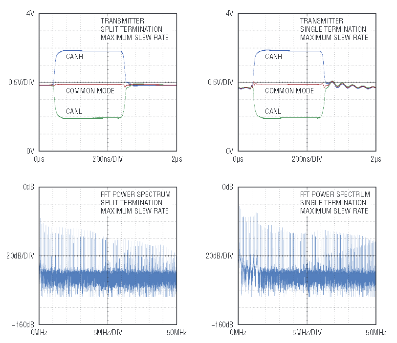
Figure 4. Transmitter waveforms and FFT power spectrum plots of the common mode voltage for split and single bus terminations on 10m unshielded twisted pair cable; VCC = 3.3V, 1Mbps
The FFT power spectra of the common mode voltage waveforms are also shown in Figure 4. The results using split termination and those using single resistor termination are both shown. The waveforms with the single resistor termination show a larger magnitude of common mode transients during the switching transition, as well as a damped oscillation after the dominant to recessive transition. This damped oscillation is the result of the inductance of the line interacting with line and transceiver capacitance after the transceiver switches to its high impedance recessive state.
In this example, the common mode voltage in the recessive state with the single resistor termination is loaded only by the four 40kΩ input resistors of two LTC2875 devices, one on each end of the cable, for a parallel resistance of 10k. By contrast, the common mode voltage in the split termination case is also loaded by the four 60Ω split termination resistors, for a parallel resistance of 15Ω, in series with two parallel 4.7nF capacitors. The common mode voltage FFT power spectrum is lower in amplitude across a wide range of frequencies for the split termination compared to the single resistor termination.
For transmitting at a lower data rate, a slower slew rate may be used for additional reduction in common mode EME. Figure 5 illustrates fourcases with minimum and maximum slew rates, combined with split or single resistor termination. These measurements were performed with the same test configuration as those shown in Figure 4, except that the data rate was reduced to 100kbps and waveforms at both the minimum and maximum slew rates were recorded.
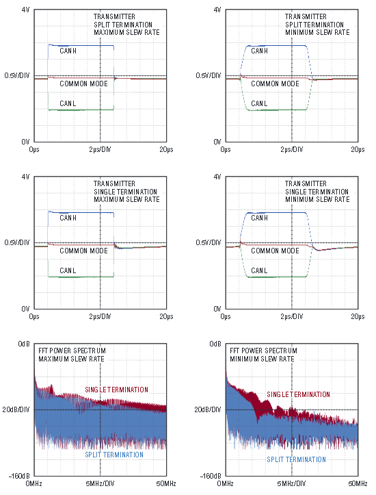
Figure 5. Transmitter waveforms and FFT power spectrum plots of the common mode voltage for four combinations of termination and slew rate; VCC = 3.3V, 100kbps, 10m unshielded twisted pair cable
As in the 1Mbps waveforms of Figure 4, the use of the split termination results in a significant reduction in common mode noise across the frequency spectrum when transmitting at 100kbps. At these lower data rates, further reductions in the common mode noise spectrum can be obtained by setting the LTC2875 to its minimum slew rate. In this example, combining both the split termination and the minimum slew rate reduces the common mode noise power by 20dB or more over most of the recorded spectrum, compared to the single resistor termination combined with the maximum slew rate.
Reducing Eme With A Common Mode Choke
Another technique to reduce EME from common mode voltage fluctuations is using a common mode choke. The choke increases the source impedance of the common mode signal, and in conjunction with capacitors added between CANH and CANL and GND, forms a lowpass filter that attenuates high frequency noise. The effectiveness of a 100μH common mode choke in conjunction with two 33pF capacitors in reducing the common mode noise is shown in Figure 6. In this example, VCC = 3.3V, split termination was employed, the twisted pair cable was 10 meters long and the data rate was 100kbps.
Mixed 3.3V And 5V Operation
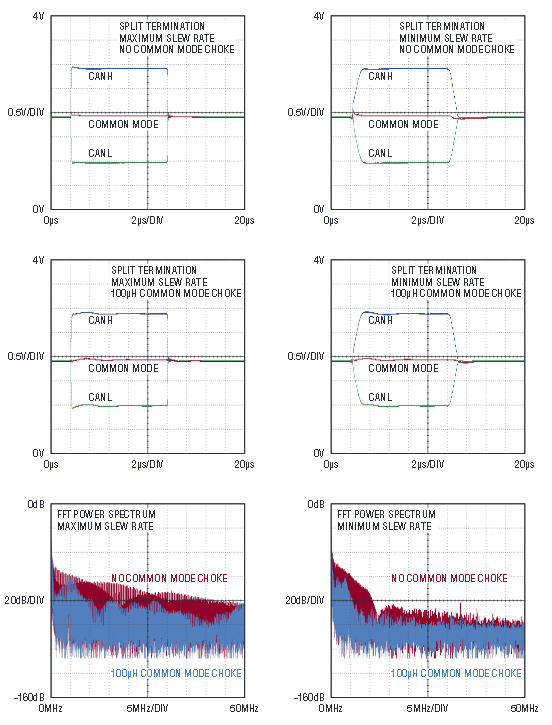
Figure 6. Transmitter waveforms and FFT power spectrum plots of the common mode voltage, with or without common mode choke
The LTC2875 transceivers operating from a 3.3V supply can interoperate with other CAN transceivers operating from a 5V supply on the same bus. The only major difference between operating at 3.3V and 5V is that the common mode voltages are ~1.95V and ~2.5V, respectively. The common mode of the bus therefore fluctuates depending on the logical state of the bus.
When all transmitters are in the recessive state, the common mode voltage settles to some intermediate voltage depending on all the resistive loads placed on the bus, including receiver input resistors, and split termination resistors (if present). When a transmitter powered by 5V is dominant, it pulls the common mode voltage toward 2.5V. When a transmitter is powered by 3.3V, it pulls the common mode voltage toward 1.95V. The common mode voltage fluctuates between 2.5V and 1.95V, resulting in a modest increase in EME.
An example of mixed voltage operation is shown in Figure 7. The experimental setup consists of two LTC2875 transceivers, each connected to the end of a 10-meter twisted pair, with split termination employed. Each transceiver alternates in driving a dominant state on the bus. The waveforms are recorded on the CANH and CANL pins of the near side transceiver.
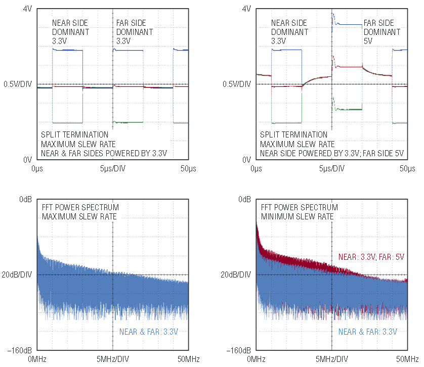
Figure 7. Transmitter waveforms and FFT power spectrum plots of the common mode voltage for two transmitters powered by identical and mixed power supply voltages; 10m unshielded twisted pair cable, 100kbps, maximum slew rate
In the plots shown on the left, both the near and far transceivers are powered by a 3.3V supply. The common mode voltage remains near 1.95V with only minor perturbations. In the plots on the right, by comparison, the near transceiver remains powered by 3.3V, while the far transceiver is powered by 5V. The recessive common mode voltage settles to about 2.23V, the average of 2.5V and 1.95V. When the near side transceiver is dominant, the common mode voltage is pulled down close to 1.95V, whereas when the far side transceiver is dominant, the common mode voltage is pulled close to 2.5V.
The difference in EME resulting from common mode voltage fluctuations can be seen by comparing the FFT power spectra of the common mode voltage recorded at the terminals of the near transceiver. An increase in power of approximately 8dB is observed from 0MHz to 25MHz for the mixed power supply voltage case, with the difference rolling off above that frequency.
±36V Common Mode Voltage Range
Standard CAN bus transceivers operate over a limited common mode voltage range that extends from −2V to +7V. In commercial or industrial environments, ground faults, noise, and other electrical interference can induce common mode voltages that greatly exceed these limits. An ideal CAN bus transceiver would survive large common mode voltages and continue to send and receive data without disruption. Accordingly, the receiver in the LTC2875 is designed to operate over an expanded ±36V common mode voltage range when operating from a 5V supply, and ±25V when operating from a 3.3V supply.
The receiver uses low offset bipolar differential inputs, combined with high precision resistor dividers, to maintain precise receiver thresholds over the wide common mode voltage range. The transmitters operate up to the absolute maximum voltages of ±60V, and will sink or source current up to the limits imposed by their current limit circuitry.
Hot Plugging, Hot Swapping, And Glitch-Free Power-Up And Power-Down
The LTC2875 features glitch-free power-up and power-down protection to meet hot plugging (or hot swap) requirements. These transceivers do not produce a differential disturbance on the bus when they are connected to the bus while un-powered, or while powered but disabled. Similarly, these transceivers do not produce a differential disturbance on the bus when they are powered up in the disabled state while already connected to the bus. In all of these cases the receiver output RXD remains high impedance (with an internal 500k pull-up resistor), while the CANH and CANL outputs remain in the high impedance recessive state.
If the transceiver is powered up in the enabled state, the chip goes active shortly after the supply voltage passes through the transceiver’s internal power good detector threshold. The RXD output reflects the state of the bus data when the chip goes active, while the transmitter remains in the recessive state with its outputs high impedance until the first recessive-to-dominant transition of TXD after the chip goes active.
If the transmitter is in the enabled state when the chip is powered down, the chip goes inactive shortly after the supply voltage passes through the transceiver’s internal supply undervoltage detector threshold. If the transmitter is in thedominant state at this time, the outputs smoothly switch to the recessive state. Regardless of whether it is outputting adominant or recessive state, the receiver output RXD smoothly switches to a high impedance state (weakly pulled upthrough an internal 500k pull-up resistor).
±60V Fault And ±25Kv Esd Tolerance
CAN bus wiring connections in industrial installations are sometimes made by connecting the bare twisted wire to screw terminal blocks. The apparatus containing the CAN bus interface may house circuits powered by 24V AC/DC or other voltages that are also connected with screw terminals. The handling of exposed wires and screw terminals by service personnel introduces the risk of ESD damage, while the possibility of wiring the cables to the wrong screw terminals introduces the risk of overvoltage damage. The high fault voltage and ESD tolerance make the LTC2875 exceptionally resistant to damage from these hazards.
The ±60V fault protection of the LTC2875is achieved by using high voltage BiCMOS integrated circuit technology. The naturally high breakdown voltage of this technology provides protection in powered-off and high impedance conditions. The driver outputs use a progressive foldback current limit design to protect against overvoltage faults while still allowing high current output drive. The LTC2875 is protected from ±60V faults even with GND open, or VCC open or grounded.
The LTC2875 is protected from electrostatic discharge from personnel or equipment up to ±25kV (HBM) to the A, B, Y and Z pins with respect to GND. On-chip protection devices begin to conduct at voltages greater than approximately ±78V and conduct the discharge current safely tothe GND pin. Furthermore, these devices withstand up to ±25kV discharges even when the part is powered up and operating without latching up. All the other pins are protected to ±8kV (HBM).
Conclusion
The LTC2875 is a groundbreaking ±60V overvoltage tolerant CAN bus transceiver that operates from either 3.3V or 5V supplies. Its industrial robustness is matched by superior performance, application flexibility and excellent EME characteristics.
