
MAXREFDES1294



概览
设计资源
描述
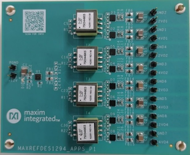
The MAXREFDES1294 is an isolated DC-DC power supply that delivers four 24V outputs and four 12V outputs from a 12V supply voltage. It is designed for an industrial system which needs multiple isolated voltages from a 12V input voltage. The MAXREFDES1294 show the techniques using the H-bridge transformer driver to generate multiple isolated outputs. This document explains how the MAX13256 can be used to deliver four 24V outputs and four 12V outputs from a 12V supply voltage.
The MAX13256 is a small, high-performance transformer driver, ideal for isolated power delivery in the industrial or medical environments. The MAX13256 is an unregulated DC-DC circuit component, that is, it has no feedback to control the secondary voltage. For this reason, the MAX13256 can be used especially in the applications where the secondary power does not need tight regulation. Even when good regulation is requested, following a MAX13256 with a post regulator can still be a cost-competitive solution.
The MAX13256 H-bridge transformer driver provides a simple solution to make isolated power supplies up to 10W. The device drives a transformer’s primary coil with up to 300mA of current from a wide 8V to 36V DC supply. The transformer’s secondary-to-primary winding ratio defines the output voltage, which allows to select any isolated output voltage virtually.
优势和特点
- Undervoltage Lockout
- 2.5V to 5V Compatible Logic Interface
- Internal or External Clock Source
- Adjustable Overcurrent Threshold
- Fault Detection and Indication
- Overcurrent Limiting
- Overtemperature Protection
- Small 10-Pin TDFN Package (3mm × 3mm)
所用产品
详情
The MAXREFDES1294 is an isolated DC-DC power supply that delivers four 24V outputs and four 12V outputs from a 12V supply voltage. It is designed for an industrial system which needs multiple isolated voltages from a 12V input voltage. The MAXREFDES1294 show the techniques using the H-bridge transformer driver to generate multiple isolated outputs. This document explains how the MAX13256 can be used to deliver four 24V outputs and four 12V outputs from a 12V supply voltage. An overview of the design specification is shown in the Table 1.
The MAX13256 is a small, high-performance transformer driver, ideal for isolated power delivery in the industrial or medical environments. The MAX13256 is an unregulated DC-DC circuit component, that is, it has no feedback to control the secondary voltage. For this reason, the MAX13256 can be used especially in the applications where the secondary power does not need tight regulation. Even when good regulation is requested, following a MAX13256 with a post regulator can still be a cost-competitive solution.
The MAX13256 H-bridge transformer driver provides a simple solution to make isolated power supplies up to 10W. The device drives a transformer's primary coil with up to 300mA of current from a wide 8V to 36V DC supply. The transformer's secondary-to-primary winding ratio defines the output voltage, which allows to select any isolated output voltage virtually.
Other features include the following:
- Undervoltage Lockout
- 2.5V to 5V Compatible Logic Interface
- Internal or External Clock Source
- Adjustable Overcurrent Threshold
- Fault Detection and Indication
- Overcurrent Limiting
- Overtemperature Protection
- Small 10-Pin TDFN Package (3mm × 3mm)
This reference circuit consists of the MAX13256 H-bridge transformer driver to demonstrate a multiple DC outputs application. The power supply delivers four 24V outputs and four 12V outputs from a 12V supply voltage. Table 1 is an overview of the design specification.
| Parameter | Symbol | Min | TYP | Max |
| Input Voltage | VIN | 11.76V | 12V | 12.24V |
| Frequency | fSW | 255kHz | 425kHz | 700kHz |
| Output Voltage | VOUT1, VOUT2, VOUT3, VOUT4 | 21.6V | 24V | 26.4V |
| Output Voltage Ripple | ΔVO1, ΔVO2, ΔVO3, ΔVO4 | 240mV | ||
| Output Current Range | IOUT1, IOUT2, IOUT3, IOUT4 | 0A | 30mA | |
| Output Voltage | VOUT5, VOUT6, VOUT7, VOUT8 | 10.8V | 12V | 13.2V |
| Output Voltage Ripple | ΔVO5, ΔVO6, ΔVO7, ΔVO8 | 120mV | ||
| Output Current Range | IOUT5, IOUT6, IOUT7, IOUT8 | 0A | 35mA | |
| Output Power | POUT | 0W | 4.56W | |
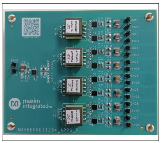
This document describes the hardware shown in the Figure 1. It provides a detailed technical guide to design a multiple isolated output DC-DC converter using Analog Device's MAX13256 H-bridge transformer driver. The power supply has been built and tested.
H-Bridge Transformer Driver and Full-wave Bridge Rectifier
A circuit known as a H-bridge because of its topological resemblance to the letter 'H', generally operates on a single voltage power supply and can apply positive or negative voltage to a load connected across the bridge. The bridge elements are often MOSFETs, which are used to make ideal electronic switches. Although linear variable conductance is sometimes used, the MOSFETs generally operate digitally either ON with a resistance in the milliohm range or OFF with a resistance in the hundreds to thousands of megohms. The pulse-width modulation (PWM) is often used to vary the power to the load linearly. A common application is to drive a DC motor at variable speed either forwards or backwards by changing the polarity of the voltage. In this reference design, a H-bridge is used to drive a transformer.
A simple H-bridge used to drive a transformer is shown in the Figure 2, which uses mechanical switches. In a real H-bridge these switches are replaced by MOSFETs. A positive voltage is applied to the transformer when switches 2 and 3 are ON. A negative voltage is applied to the transformer when switches 1 and 4 are ON. It is critical that switches 1 and 2 or switches 3 and 4 are never ON at the same time. In this case, a very high current from the power source and the destruction of the switches is possible.
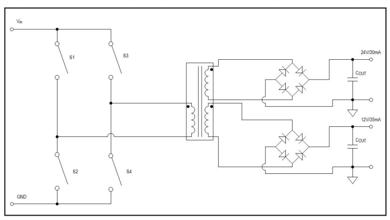
In a typical application, switches 1 and 3 are used to control the polarity of the voltage applied to the transformer, and one or the other is always ON. A PWM waveform is then applied to either switch 2 or switch 4 to control the power to the transformer. It should be noted that although the average voltage across the transformer is a linear function of the PWM duty cycle, the average voltage cannot be used in calculating power to the transformer for the square of the average voltage is not the same as the square of the rms voltage. However, the average power delivered to the transformer is a linear function of the PWM duty cycle.
Full-Wave Bridge Rectifier Introduction
The full-wave bridge rectifier uses four individual rectifying diodes connected in a closed loop "bridge" configuration to produce the desired output.
The main advantage of this bridge circuit is that it does not require a special center tapped transformer, thereby reducing its size and cost. The single secondary winding is connected to one side of the diode bridge network and the load to the other side as shown in the Figure 3.
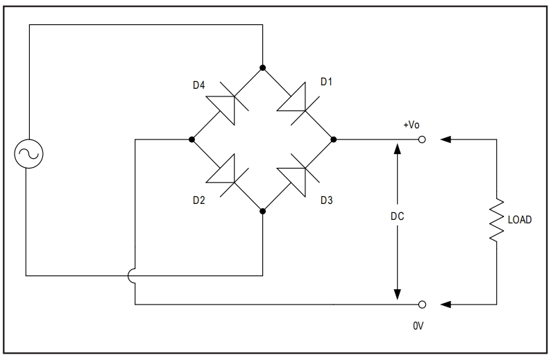
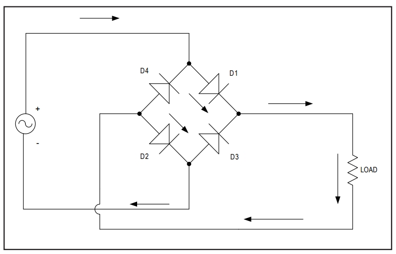
The four diodes labelled D1 to D4 are arranged in a "series pairs" with only two diodes conducting current during each half cycle. During the positive half cycle of the supply, diodes D1 and D2 conduct in series while diodes D3 and D4 are reverse biased and the current flows through the load as shown in the Figure 4.
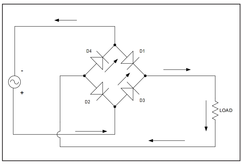
During the negative half cycle of the supply as shown in the Figure 5, diodes D3 and D4 conduct in series, but diodes D1 and D2 switch "OFF" as they are now reverse biased. The current flowing through the load is in the same direction as before.
Design Procedure for the H-Bridge Transformer Driver Converter
Now that the principle of operation of the H-bridge transformer driver and full-wave bridge rectifier are clear, a practical design example can be shown. This document is primarily concerned with the transformer design based on the datasheet of MAX13256.
The following design parameters are used throughout:
| Symbol | Function |
| VIN | Input Voltage |
| VOUT | Output Voltage |
| ΔVOUT | Output Ripple Voltage |
| IOUT | Output Current |
| POUT | Output Power |
| fSW | Switching Frequency |
| n | Primary-Secondary Turns Ratio |
| NP | Turns of Primary Winding |
| NS | Turns of Secondary Winding |
The above symbols are sometimes followed by parenthesis to indicate whether minimum or maximum values of the parameters are intended, for example, the minimum input voltage is intended by the symbol VIN(MIN); otherwise, typical values are intended. In addition, the schematic document is referred throughout the procedure.
Step 1: Choosing Secondary-Side Rectification Circuits
The MAX13256 allows a versatile range of secondary-side rectification circuits. The primary-to-secondary transformer winding ratio can be chosen to adjust the isolated output voltage. The device delivers up to 300mA of current to the transformer with a supply up to +36V. The full-wave rectifier circuit is chosen for this reference design.
Step 2: Choose the Switching Frequency
The MAX13256 includes an internal oscillator that drives the H-bridge when a watchdog timeout is detected on CLK. The outputs switch at 425kHz (typ) with a guaranteed 50% duty cycle in the internal oscillator mode.
Step 3: Overcurrent Limiting
The MAX13256 limits the ST1/ST2 output current. Connect an external resistor (RLIM) to ITH to set the current limit. When the current reaches the limit for longer than the blanking time of 1.2ms (typ), the drivers are disabled, and FAULT is asserted low. The drivers are re-enabled after the auto-retry time of 38.4ms (typ). If a continuous fault condition is present, the duty cycle of the fault current is approximately 3%. To set the current-limit threshold, use the following equation:
where ILIM is the desired current threshold in the range of 215mA < ILIM < 650mA (typ). A 1kΩ, 1% resistor is used in this reference design to set the current limit to 650mA.
Step 4: Choosing the Right Transformer with the MAX13256
The MAX13256, a 10W transformer driver, is an improved way to convey power across isolation boundaries. As with all transformer drivers, good system performance requires a good transformer specification. Though many transformers can potentially work with the MAX13256, not all transformer data sheets are specified with a transformer driver application in mind. This reference design chose the specified transformer based on the Application Note 5766.
Unlike regulated DC-to-DC architectures, the MAX13256 always drives the transformer with a 50% duty cycle square wave. Consequently, output voltages depend on transformer winding turns ratios. So, care must be taken to select or specify an appropriate transformer for each application. This reference design uses four transformers to provide eight output voltages, so specified transformers were chosen to meet high-performance requirement.
Important Parameters Affected by Transformer Specifications
Transformer specifications affect:
- Power dissipation in the MAX13256: affected by core losses and magnetizing inductance
- Power dissipation in the transformer: affected by core losses, primary resistance, magnetizing inductance, and secondary resistance
- Output voltage: affected by primary resistance and secondary resistance
- Peak output current: affected by core losses and magnetizing inductance
Calculating the Transformer Turns Ratio
For the full-wave rectifier circuit, the transformer turns ratio is given by the following expression:
where VD is the forward voltage drop of the secondary rectifier which is about 0.5V. There are four 24V outputs and four 12V outputs for this reference design, the turn ratios of the 24V and 12V outputs are,
Calculating the ET Constant
The ET product relates the maximum allowable magnetic flux density in a transformer core to the voltage across a winding and switching period. The inductor magnetizing current in the primary winding changes linearly with time during the switching period of the device. Transformer manufacturers specify a minimum ET product for each transformer. The transformer's ET product must be larger than:
where fSW is the minimum switching frequency of the ST1/ST2 outputs (255kHz (min)) when the internal oscillator is used.
Step 5: Diode Selection
The high switching speed of the MAX13256 requires high-speed rectifiers. Ordinary silicon signal diodes such as 1N914 or 1N4148 can be used for low-output current levels (less than 50mA.) But at higher output current levels, their reverse recovery times might degrade efficiency. At higher output currents, select low forward voltage Schottky diodes to improve efficiency. Ensure that the average forward current rating for the rectifier diodes exceeds the maximum load current of the circuit. To save the board space and improve the efficiency, the 0.5A SBR bridge super barrier rectifier SBR05M60BLP is used to implement the full-wave bridge rectifier circuit. The SBR05M60BLP features 0.49V low forward voltage drop and low reverse leakage current.
Step 6: Input Bypass Capacitor Selection
Bypass the supply pin to GND with at least 1μF ceramic capacitor as close as possible to the device. The equivalent series resistance (ESR) of the input capacitors is not as critical as for the output filter capacitors. Typically, ceramic X7R capacitors are adequate. A 10μF ceramic capacitor and a 0.1μF ceramic capacitor are used in this reference design to improve electromagnetic interference (EMI) performance.
Step 7: Output Filter Capacitor and Bead Selection
In most applications, the actual capacitance rating of the output filter capacitors is less critical than the capacitor's ESR. In applications sensitive to output-voltage ripple, the output filter capacitor must have low ESR. For optimal performance, the capacitance should meet or exceed the specified value over the entire operating temperature range. Capacitor ESR typically rises at low temperatures. However, OS-CON capacitors can be used at temperatures below 0°C to help reduce output-voltage ripple in sensitive applications. In applications where low output voltage ripple is not critical, standard ceramic 0.1μF capacitors are sufficient.
To improve EMI performance, a 10μF ceramic capacitor and a 1μF ceramic capacitor are used at each output. And two ferrite-bead are used at each output to absorb high frequency interference.
文件和资源
-
MAXREFDES1294 Design Files2021/11/11ZIP1M
-
MAXREFDES1294: 12VIN, Eight-output, Isolated DC-DC Power Supply Using the MAX132562021/12/15PDF561 K
支持与培训
搜索我们的知识库,获取技术问题答案。我们专门的应用工程师团队也会随时为您解答技术问题。