

概览
设计资源
描述
Analog's power supply experts have designed and built a series of isolated, industrial and medical power-supply reference designs. Each of these power supplies efficiently converts 24V or 12V into useful voltage rails at a variety of power levels. Each design has been tested for load and line regulation, as well as efficiency and transient performance.
MAXREFDES124 is an efficient no-opto flyback topology with 12V input, and a 5.5V output at 22W of power (4A). The design features the MAX17690, a peak-current-mode converter with flexible switching frequency and the MAX17606, a secondary side MOSFET driver for a flyback converter. The combination of no opto-coupler and a secondary-side MOSFET results in a design that is optimized for space, cost, and efficiency. This entire circuit fits on a 20mm (0.7874in) × 66mm (2.5984in) board.
Most boards feature through-hole pins for immediate board placement and accelerated prototyping. As with all Analog reference designs, boards are available for purchase.
优势和特点
Features
- Functional insulation
- Compact and flexible
- Minimal external components
- 5kV of isolation for medical and other high-isolation applications
- ±5% output accuracy
Competitive Advantages
- Rapid prototyping
- Accelerated design time
- Cool system operation
详情
Isolated power supplies provide reliable power regulation for a variety of applications. The MAXREFDES124# is a compact 12V input no-opto flyback converter module with secondary-side synchronous MOSFET driver that features 5.5V at 4A output. Through-hole pins on the bottom side of the module allows quick and easy integration of this power converter into the main system. Pins are 15.24mm (0.6in) from power to ground, and 50.8mm (2in) from the input side to the output side.
The MAX17690 is a no-opto peak-current-mode controller for design of wide input-voltage flyback regulators. The reference design operates over a 9V to 18V input-voltage range, and provides up to 4A at 5.5V output. The switching frequency is programmable from 50kHz to 250kHz, allowing optimization of filter components, resulting in compact and cost-effective power conversion. This design is set to switch frequency at 150kHz. No opto-coupler or third winding are needed to derive feedback signal across isolation boundary as the MAX17690 senses the isolated output voltage directly from the primary-side flyback waveform during the off-time of the primary switch.
The input undervoltage lockout (EN/UVLO) is provided for programming the input-supply start voltage, set to 7.26V in the design, and to ensure proper operation during brownout conditions. The EN/UVLO input is also used to turn on/off the IC. The overvoltage-input (OVI) protection scheme is provided to make sure that the controller shuts down when the input supply exceeds its maximum allowed value, set to 21.78V in the design.
A capacitor is connected to the SS pin to program the soft-start period hence reduces the input inrush current during startup. Hiccup-mode overcurrent protection and thermal shutdown are provided to minimize dissipation in overcurrent- and overtemperature-fault conditions.
On the secondary side, a MOSFET replaces the diode for a typical flyback converter. The MAX17606 drives the MOSFET. By replacing the secondary diode with a MOSFET, the MAX17606 improves the efficiency and reduces heat dissipation. The reference design delivers a peak efficiency of 87% with the supplied components when the input is 12V. This general-purpose power solution can be used in many different types of power applications, such as medical equipment and other high-isolation applications.
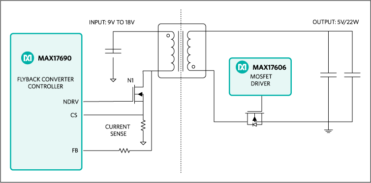
Figure 1. The MAXREFDES124 reference design block diagram
The MAXREFDES124 reference design contains all the control circuitry and components required for designing a 9V to 18V wide-input, 5.5V (22W) output isolated -flyback-converter power supply.
When the primary-side MOSFET is turned on, the current flows through the primary winding of the transformer and stores the energy. The CS-pin input and the current-sense resistor set the peak current limit and provide overcurrent protection. When the MOSFET is turned off, the energy stored in the primary side is transferred to the secondary side. The MAX17690 samples the output voltage by sensing the voltage of the transformer on the primary side.
The secondary side of the circuit consists of a MOSFET, a MAX17606 MOSFET driver, and a few output capacitors. The MOSFET emulates the diode in a typical flyback converter. The MAX17606 senses the voltage at the drain pin of the MOSFET to determine the timing of turning on/off the MOSFET. When the MOSFET on the primary side is off and the drain voltage of the MOSFET on the secondary side becomes less than -94mV, the MAX17606 turns on the MOSFET and the transformer pushes the current to the load at the output and the remaining energy is stored in the output capacitors. When the MOSFET is on and the drain voltage of the MOSFET on the secondary side becomes more than 30mV, the MAX17606 turns off the MOSFET to prevent the current flow back into the transformer and discharges the output capacitors.
The MAXREFDES124 system requires 2% of full load (about 80mA) for the output to regulate within limits. When the load is lower than 2%, the output is clamped by a 6.2V Zener diode.
Startup Voltage and Input Overvoltage Protection Setting (EN/UVLO, OVI)
The EN/UVLO pin in the MAX17690 serves as an enable/disable input, as well as an accurate programmable undervoltage lockout (UVLO) pin. The MAX17690 does not begin startup opera-tions unless the EN/UVLO -pin voltage exceeds 1.21V (typ). The MAX17690 turns off if the EN/UVLO -pin voltage falls below 1.09V (typ). A resistor-divider from the input DC-bus-to-ground can be used to divide down and apply a fraction of the input DC voltage to the EN/ UVLO pin. The values of the resistor-divider can be selected so that the EN/UVLO-pin voltage exceeds the 1.21V (typ) turn-on threshold at the desired input DC-bus voltage. The same resistor-divider can be modified with an additional resistor (ROVI) to implement OVI protection in addition to the EN/UVLO functionality. When the voltage at the OVI pin exceeds 1.21V (typ), the MAX17690 stops switching. Switching resumes with soft-start operation, only if the voltage at the OVI pin falls below 1.09V (typ). For the expected values of the startup DC-input voltage (VSTART) and OVI protection voltage (VOVI), the resistor values for the divider can be calculated as follows:
VSTART = (R5 + R6 + R7)/(R5 + R6) × 1.21 (V)
VOVI = (R5 + R6 + R7)/R5 × 1.21 (V)
If R5 = 10kΩ, R6 = 20kΩ, and R6 = 150kΩ, then:
VSTART = 7.26V, VOVI = 21.78V.
The MAXREFDES124 board is fully assembled and tested. Use the following steps to verify board operation.
- Turn off the power supply.
- Connect the positive terminal of the power supply to the VIN pin of the MAXREFDES124 board.
- Connect the negative terminal of the power supply to the PGND pin of the MAXREFDES124 board.
- Connect the VOUT connector of the MAXREFDES124# board to the positive terminal of the electronic load.
- Connect the negative terminal of the electronic load to the positive terminal of the ammeter.
- Connect the negative terminal of the ammeter to the GNDO connector of the MAXREFDES124 board.
- Connect the voltmeter across the VOUT and the GNDO connectors of the MAXREFDES124 board.
- Turn on the power supply.
- Set the electronic load to a constant current between 80mA to 4000mA.
- Verify the second voltmeter reading is 5.5V ±0.275V.
Lab Measurements
The MAXREFDES124 design was verified and tested under full input range and different output load conditions. The power efficiency vs. load current is illustrated in Figure 2.

Figure 2. Power efficiency vs. load current.
Figure 3 displays the output ripple at full load when the input is 12V.

Figure 3. Output ripple at 4A load, 5.5Vout
Figure 4 displays the load transient response when the load is stepped from 5mA to 1.6A, and then dropped back to 5mA again. The output transient spike is about 1V. The input is 12V and output is 5.5V.

Figure 4. Transient response when load steps from 5mA to 1.6A
Figure 5 shows the load transient response when the load is stepped from 2.4A to 4A, and then dropped back to 2.4A again. The transient voltage is about 200mV. The input is 12V, and the output is 5.5V.
Figure 5. Transient response when load steps from 2.4A to 4A
Required Equipment:
- MAXREFDES124 board
- One 12V -DC power supply
- One electronic load
- 1 voltmeter
- 1 ammeter
文件和资源
-
MAXREFDES124 Design Files2021/2/15ZIP15 M
支持与培训
搜索我们的知识库,获取技术问题答案。我们专门的应用工程师团队也会随时为您解答技术问题。