
MAXREFDES1198


概览
设计资源
描述
The MAX17632 family of parts (MAX17632A, MAX17632B, and MAX17632C) includes high-efficiency, high-voltage, synchronous step-down DC-DC converters with integrated MOSFETs operating over an input-voltage range of 4.5V to 36V. These parts can deliver current up to 2A. The MAX17632A and MAX17632B are fixed 3.3V and fixed 5V output parts, respectively. The MAX17632C is an adjustable output voltage (0.9V to 90% of VIN) part. Built-in compensation across the output-voltage range eliminates the need for external compensation components. The MAX17632 features peak-current-mode control architecture. The device can be operated in forced pulse width modulation (PWM), pulse-frequency modulation (PFM), or discontinuous-conduction mode (DCM) to enable high efficiency under full-load and light-load conditions.
优势和特点
- Wide 4.5V to 36V Input
- 3.3V Output
- Up to 2A Output Current
- Fully Assembled and Tested
- Proven PCB Layout
所用产品
详情
The MAX17632 family of parts (MAX17632A, MAX17632B, and MAX17632C) includes high-efficiency, high-voltage, synchronous step-down DC-DC converters with integrated MOSFETs operating over an input-voltage range of 4.5V to 36V. These parts can deliver current up to 2A. The MAX17632A and MAX17632B are fixed 3.3V and fixed 5V output parts, respectively. The MAX17632C is an adjustable output voltage (0.9V to 90% of VIN) part. Built-in compensation across the output-voltage range eliminates the need for external compensation components.
The MAX17632 features peak-current-mode control architecture. The device can be operated in forced pulse width modulation (PWM), pulse-frequency modulation (PFM), or discontinuous-conduction mode (DCM) to enable high efficiency under full-load and light-load conditions. Key features of this design include the following:
- Wide 4.5V to 36V Input
- 3.3V Output
- Up to 2A Output Current
- Fully Assembled and Tested
- Proven PCB Layout
This design is a single-output, synchronous buck, stepdown DC-DC converter for small size and low output voltage. Table 1 provides an overview of the design specification.
| Parameter | Symbol | Min | Max |
| Input Voltage | VIN | 4.5V | 36V |
| Frequency | fSW | 400kHz | |
| Maximum Efficiency | η | 91% | |
| Output Voltage | VOUT | 3.3V | |
| Output Voltage Ripple | ΔVOUT | 33mV | |
| Output Current | IOUT | 0 | 2A |
| Output Power | POUT | 6.6W | |
Hardware Needed for Quick Setup
- 4.5V to 36V, 10A DC input power supply
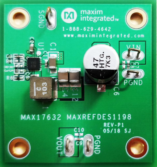
- MAXREFDES1198 board
- Load capable of sinking 5A
- Digital voltmeter (DVM)
This document provides a detailed systematic technical guide for the design of a buck converter using the MAX17632 for smaller size. Refer to the MAX17632 IC data sheet and MAX175632A EV kit data sheet for device operation details. The converter design has been built and tested, details of which follow later in this document.
The buck power converter is a DC-DC converter whose output voltage is less than the input voltage. This is a non-isolated topology, which means the input and output share a common ground. Figure 2 shows the basic circuit of the synchronous buck power converter. The difference between synchronous buck and traditional buck is that in a synchronous buck, a transistor NL is placed in parallel to the diode to reduce the voltage drop and, therefore, to increase the efficiency.
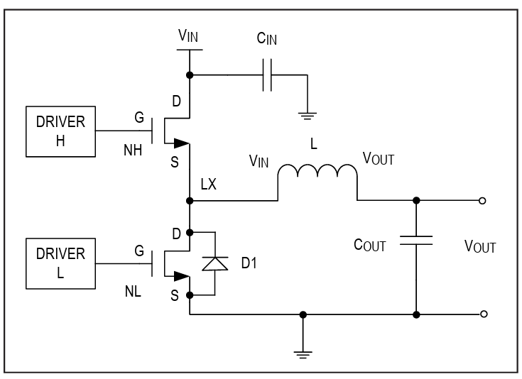
A buck power converter has the following components:
- Input capacitor (CIN) and output capacitor (COUT)
- A switch, in this case a transistor NH
- An energy storage element, inductor (L)
- Transistor NL and diode D1 to conduct during the off-state of the switch
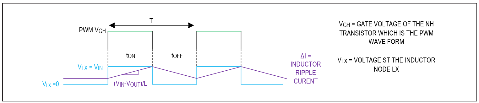
Figure 3 shows the basic operation of the buck power converter. During the on-state (tON) of the transistor NH, the voltage at the node LX is equal to VIN and then the current across the inductor rises linearly at a rate of (VIN - VOUT)/L. When the transistor NH is off (tOFF), the voltage at the LX node is 0V and the current in the inductor falls linearly. It is the property of the inductor to maintain the flow of the current, so this reverses the polarity of the inductor during the NH off-state. The current through the inductor never falls to zero. This is called Continuous Conduction Mode (CCM). The ripple current ∆I is an important parameter that is approximately 20 percent to 50 percent of IL(load current).
Now that the theory behind the synchronous buck is explained, a practical design technique can now be illustrated. The design procedure involves the following stages: output voltage selection, inductor and capacitor selection, and setup of the switching frequency. This document is intended to complement the information contained in the MAX17632 IC data sheet.
| Symbol | Function |
| VIN | Input voltage |
| VFB | Feedback threshold voltage |
| VOUT | Output voltage |
| ΔVOUT | Output ripple voltage |
| IOUT | Output current |
| η | Target minimum efficiency |
| PIN | Input power |
| fSW | Switching frequency |
| D | Duty cycle |
The following design parameters are used throughout:
Step 1: Setting the Output Voltage
The MAX17632’s output voltage can be adjusted between 0.9V and 0.9 × VIN. The output using the R3 and R4 resistors connected to the FB pin is calculated as follows:

In this design since the output voltage is 3.3 volts we are considering R3 = 0Ω and R4 = open circuit. Refer to Typical applications circuits in MAX17632 data sheet.
Step 2: Setting the Switching Frequency
The MAX17632 can operate between 400kHz and 2.2MHz. The RT pin is used to set the regulator’s switching frequency. The RT pin is left unconnected, which defaults to 400kHz. This is calculated using the following formula:

where RRT is in kΩ and fSW is in kHz. The switching frequency fSW = 400kHz is chosen here.
Step 3: Selecting the Output Inductor
The LX pin is connected to the switching node of the inductor. The value of the inductor is calculated as follows:

where VOUT = 3.3V, fSW = 400kHz, and L = 6.8µH are chosen for this design.
Step 4: Selecting the Output and Soft-Start Capacitor
The soft-start feature ramps up the output voltage slowly, reducing input inrush current during startup. A capacitor connected from SS to SGND determines the soft-start. This soft capacitor depends upon the output capacitor. The output capacitance can be calculated as follows:

where ISTEP is the load current step, tRESPONSE is the response time of the controller, ∆VOUT is the allowable output voltage deviation, fC is the target closed-loop crossover frequency, and fSW is the switching frequency. Choose fC to be 1/10 of fSW because in this design the switching frequency is less than 800kHz (refer to the MAX17632 data sheet for more information).
Substitute the following values in the above equations:
ISTEP = 1A
∆VOUT = 0.33V
fC = (400k/10)
fSW = 400kHz
tRESPONSE = 8.3µs
COUT = 42µF
Hence, two 22µF capacitors are selected in parallel for the nominal value.
The soft-start capacitance (CSS) is calculated as follows:
CSS ≥ 28 x 10-6 × COUT × VOUT
COUT is the selected output capacitance:
CSS ≥ 28 x 10-6 × 44 × 10-6 × 4
where CSS ≥ 4.066nF. CSS = 5600pF is considered the nominal value.
Step 5: Setting the Undervoltage Lockout (UVLO)
UVLO is a technique used to shut down the power to the IC when the input voltage is less than operational value. R1 and R2 are used to set the UVLO of the converter. In this design the pin is connected to VIN pins for always-on operation.
Step 6: Compensation
The MAX17632 is internally compensated.
Step 7: Input Capacitor Selector
The input filter capacitor reduces peak currents drawn from the power source and reduces noise and voltage ripple on the input caused by the circuit’s switching. The input capacitor RMS current requirement (IRMS) is defined by the following equation:

Substituting the values:
IOUT(MAX) = 2A
VIN = 24V
VOUT = 3.3V
IRMS = 0.688A
Calculate the input capacitance using the following equation:

Substituting the values:
IOUT(MAX) = 2A

η = 91%
fSW = 400kHz
∆VIN = 45mV
where the input capacitor = 2.2µF. As suggested in the data sheet page 19 input capacitor selection an electrolytic capacitor of 47µF is added in parallel.
文件和资源
-
MAXREFDES1198 Design Files2021/2/16ZIP1 M
支持与培训
搜索我们的知识库,获取技术问题答案。我们专门的应用工程师团队也会随时为您解答技术问题。