Design Note 17: Programming Pulse Generators for Flash Memories
Recently introduced “flash” memories add electrical chip-erasure and reprogramming to established EPROM technology. These features make them a cost effective and reliable alternative for updatable non-volatile memory. Utilizing the electrical program-erase capability requires linear circuitry techniques. The Intel 28F256 flash memory, built on the ETOX process, specifies programming operation with 12V or 12.75V (faster erase/program times) amplitude pulses. These “VP-P” amplitudes must fall within 1.6%, and excursions beyond 14.0V will damage the device.
Providing the VP-P pulse requires generating and controlling high voltages within the tightly specified limits. Figure 1’s circuit does this. When the VP-P command pulse goes low (trace A, Figure 2) the LT1072 switching regulator drives L1, producing high voltage. DC feedback occurs via R1 and R2, with AC roll-off controlled by C1 and R3-C2. The result is a smoothly rising VP-P pulse (trace B) which settles to the required value. The specified R1 values allow either 12V or 12.75V outputs. The 5.6V zener permits the output to return to 0V when the VP-P command goes high. It may be deleted in cases where a 4.5V minimum output is acceptable (see Intel 28F256 data sheet). The 0.1% resistors combine with the LT1072’s tight internal reference to eliminate circuit trimming requirements. Additionally, this circuit will not spuriously overshoot during power-up or down.
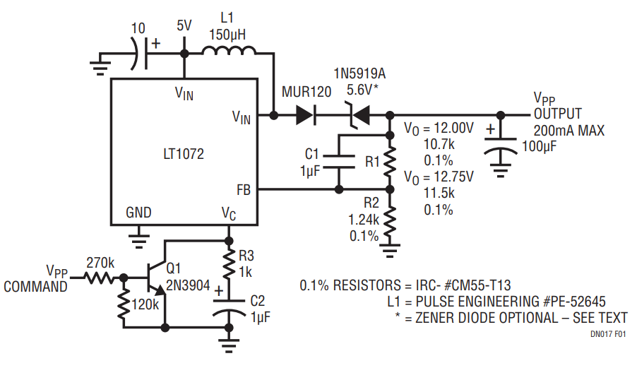
Figure 1. Basic Flash Memory VPP Pulse Generator.
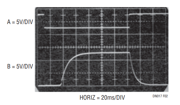
Figure 2. Waveforms for Basic Flash Memory Pulser.
Figure 1’s repetition rate is limited because the regulator must fully rise and settle for each VP-P command. Figure 3’s circuit serves cases which require higher repetition rate VP-P pulses. Here, the switching regulator runs continuously, with the VP-P pulses generated by the A1-A2 loop. If desired, the “VP-P Lock” line can be driven, shutting down the regulator to preclude any possibility of inadvertent VP-P outputs. When VP-P Lock goes low (trace A, Figure 4) the LT1072 loop comes on (trace B), stabilizing at about 17V. Pulsing the VP-P command line low causes the 74C04 (trace C) to bias the LT1004 reference. The LT1004 clamps at 1.23V with A1 and A2 giving a scaled output (trace D). The 680pF capacitor controls loop slewing, eliminating overshoots. Figure 5 details the VP-P output. Trace A is the 74C04 output, with trace B showing clean VP-P characteristics. As in Figure 1, spurious VP-P outputs are suppressed during power-up or down. The diode path around A2 prevents overshoot during short circuit recovery.

Figure 3. High Repetition Rate VPP Pulse Generator
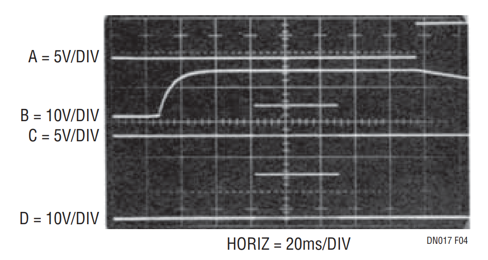
Figure 4. Operating Details of High Repetition Rate Flash Memory Pulser.
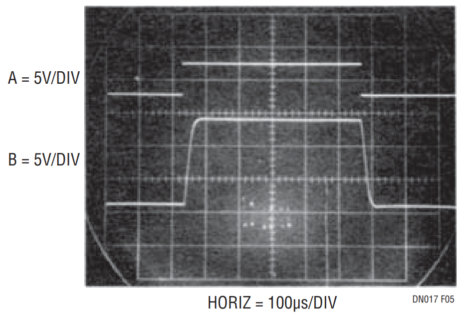
Figure 5. Expanded Scale Display of Figure 3’s VPP Pulse. Controlled Risetime Eliminates Overshoots.
A good question might be; “Why not set the switching regulator output voltage at the desired VP-P level and use a simple low resistance FET or bipolar switch?” Figure 6 shows that this is a potentially dangerous approach. Figure 6a shows the clean output of a low resistance switch operating directly at the VP-P supply. The PC trace run to the memory chip looks like a transmission line with ill-defined termination characteristics. As such, Figure 6a’s clean pulse degrades and rings badly (Figure 6b) at the memory IC’s pins. Overshoot exceeds 20V, well beyond the 14V destruction level. The controlled edge times of the circuits discussed eliminate this problem. Further discussion of these and other circuits appears in LTC Application Note 31, “Linear Circuits for Digital Systems” (Available February, 1989).
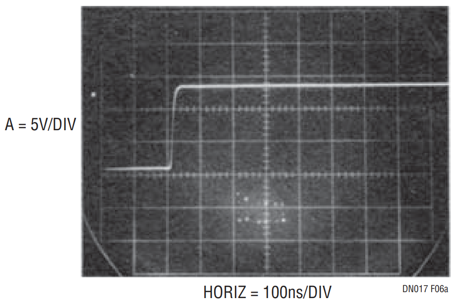
Figure 6a. An “Ideal” Flash Memory VPP Pulse.
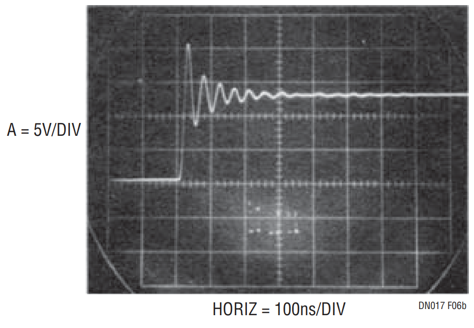
Figure 6b. Rings at Destructive Voltages After a PC Trace Run.
作者
