Bit Error Rate Testing the DS314x Series of DS3/E3 Framers
Abstract
This application note shows how to connect our enhanced bit error-rate tester (BERT) to our DS3/E3 framer using a ITU O.151 pattern in ungapped clock mode.
Introduction
This application note demonstrates how to use pattern generation, synchronization, and bit test features of the DS2174 enhanced bit error-rate tester (BERT) with the single and multiport versions of the DS314x series of DS3/E3 framers.
The DS2174 is similar to the DS2172/DS21372, but contains larger bit and error counters as well as a 512-byte random pattern buffer. It is a 3.3V device with a 1-/4-/8-bit parallel bus that allows operation in bit/nibble/byte mode. In bit mode, the clock rate can reach 155MHz (STS-1/EC-1). In byte mode, the clock rate can reach 80MHz for a net of 622Mbps (OC-3). The DS3141/2/3/4 are single, dual, triple, and quad-channel DS3/E3 framers, respectively, all of which are offered in a 144-pin, 13mm x 13mm CSBGA package. The DS3146/8/12 are 6-, 8-, and 12-channel DS3/E3 framers, respectively, and are offered in a 349-pin, 27mm x 27mm BGA package.
Each framer package keeps the same pinout across its own series. Thus, a printed circuit board (PC board) with the 349-pin BGA footprint can be populated for 6-, 8-, or 12-channel framers, depending on the device installed. Likewise, if the PC board has the 144-pin footprint, it can support 1-, 2-, 3-, or 4-channel framers.
One difference the DS3146/8/12 has over the DS3141/2/3/4 is that the main input clock to each framer can be configured as 6, 8, or 12 separate clocks or as one constant clock across all framers. If the TCSEL input pin is wired low, then the TICLKn pin expects a separate transmit input clock to each framer. If one constant clock is to be used, then TCSEL should be wired high with TICLKn wired low.
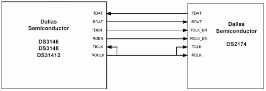
Figure 1 shows a typical configuration of a separate transmit input clock to one of the slices on the DS3146/8/12 framer that is connected to the DS2174 in ungapped clock mode. The framer is sending a 223 - 1 ITU O.151 compliant pseudorandom pattern to the BERT, and independently the BERT is sending the same pattern back. Both devices are in E3 mode.

Figure 1. Ungapped clock mode BERT and framer bidirectional synchronization.
The register settings needed to perform the illustrated configuration are as follows:
DS3146/8/12 Registers
Apply a 34.368MHz clock to the TICLK pin. Clear the TUA1 bit in MC1. Clear the RDATH bit in MC4. Set BENA, TINV, and RINV bits in BCR1. Toggle the LC bit high, then low. Set PS2 in BCR2.
DS2174 Registers
Clear the TINV and RINV bits in CR2. Set the SEED bit in CR4. Write 0xFF to registers TS0?3. Now clear the SEED bit. Write 0x42 to TS2. Load the transmit shift register by toggling high, then low, the TL bit in CR1. Then toggle LC as well in CR1.
You should now see the BERT synched to the framer (SR = 0x01). Next toggle RESYNC in BCR1 on the framer, and the framer should now be synched to the BERT (BSR = 0x01).
DS2174/DS314x Information
If you have further questions on how to connect the DS2174 EBERT with any framer within the DS314x series, please contact the Telecommunication Applications support team.