Add Margining Capability to a DC/DC Converter
Abstract
You can easily add margining capability (digital adjustment of the output voltage) to a DC/DC converter by adding a 2- or 4-channel, I2C-adjustable current DAC (DS4402 or DS4404) at the converter's feedback input. Because each DAC output is 0mA at power up, the extra circuitry is transparent to the system until a command is written via the I2C bus.
Introduction
A similar version of this article appeared in the September 18, 2008 issue of EDN magazine.
You can easily add margining capability to a DC/DC converter (digital adjustment of the output voltage) by making a single connection to the existing circuit as shown by the dotted line in Figure 1. The extra IC is a 2- or 4-channel, I2C-adjustable current DAC (DS4402 or DS4404). Because each DAC output is 0mA at power up, the extra circuitry is essentially transparent to the system until a command is written via the I2C bus.

Figure 1. Circuitry on the right, added to the feedback input of a DC/DC converter, adds margining capability to the converter.
As an example, assume VIN = 3V to 5.5V, VOUT = 1.8V (the desired nominal output voltage), and VFB = 0.6V (not to be confused with VREF of the DS4404). You can obtain the VFB value from the DC/DC converter datasheet, being sure to verify that it is within the OUTx voltage range specified in the current DAC datasheet (specified as VOUT:SINK and VOUT:SOURCE depending on whether you are sinking or sourcing current). It's also important to verify the input impedance of the DC/DC converter's FB pin (the circuit shown assumes a high impedance).
Assume we want to add a ±20% margining capability to the DC/DC converter output (VOUT):
VOUTMAX = 2.16V
VOUTNOM = 1.8V
VOUTMIN = 1.44V
First, determine the necessary relationship between RTOP and RBOTTOM that yields the nominal output (VOUTNOM) when IDS4404 = 0A:

Solving for RTOP,

For our example,

The current (IDS4404) required to make VOUT increase to VOUTMAX is derived by summing currents at the FB node:

This equation can be simplified by solving Equation 1 for RBOTTOM and substituting, which yields:

In terms of margin percentage:
where margin = 0.2, to implement ±20% margining in this case. Before you can use this relationship to calculate RTOP and RBOTTOM, you must select the full-scale current IFS.
According to the DS4404 datasheet, the full-scale current (specified as IOUT:SINK or IOUT:SOURCE) must be between 0.5mA and 2.0mA, to guarantee the specifications for accuracy and linearity. Unfortunately, no formula is available for calculating the ideal full-scale current. That value is influenced by the desired number of steps, the step size, and the values for RTOP and RBOTTOM. Another factor affecting the full-scale current value would be the requirement that a particular register setting correspond to a particular margin percentage.
In any case, your selection of a full-scale current will likely require several iterations, in which you select an arbitrary value (within the range), and then calculate RTOP, RBOTTOM, RFS, and step size. When you've determined an acceptable full-scale current value, you may want to further adjust it (or some of the resistor values) to ensure that the resistor values finally specified are commonly available.
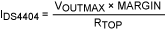
To calculate RTOP for the original example, we choose IFS = IDS4404, which gives us 31 equal increments (steps) from VOUTNOM to VOUTMAX, as well as 31 steps from VOUTNOM to VOUTMIN. This resolution is more than adequate for our example. We could, for instance, begin by arbitrarily choosing IFS in the center (1.25mA) of the specified range, and then performing all the calculations. Instead, for illustrative purposes we perform calculations for the endpoints of the range (0.5mA, 2.0mA).
So, for IFS = IDS4404 = 0.5mA: Using Equation 3 and solving for RTOP,

To calculate RFS, use the formula in the DS4404 datasheet plus the VREF value also found in that datasheet:

Finally, for completeness we determine the DS4404 output current as a function of register setting: IOUT(register setting) = step size × register setting.
Note that the register setting above does not include the sign bit, which is used to select sink or source. The DS4404 sinks current when the sign bit = 0, making VOUT increase to VOUTMAX. It sources current when the sign bit = 1, making VOUT decrease towards VOUTMIN.
For IFS = IDS4404 = 2.0mA:

Comparing RTOP and RBOTTOM for the two cases (IFS = 0.5mA vs. 2.0mA), you can see that IFS = 0.5mA is more attractive because the resistances are higher.