AN-1515: 利用ADG1211开关实现采样保持电路
电路功能与优势
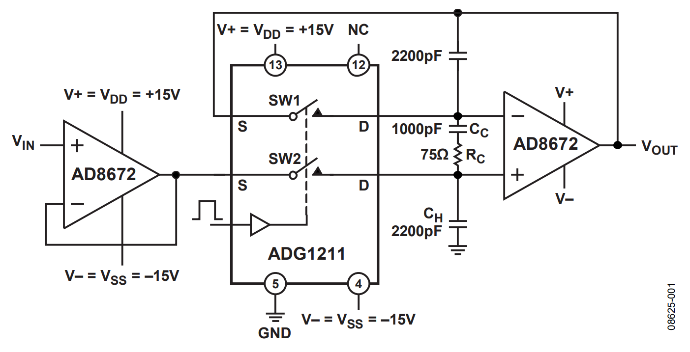
图1所示电路具有采样保持放大器(SHA)功能,SHA是数据采集和模数转换过程的基础。在一些可编程逻辑控制器(PLC)输出模块中,每通道均有采样保持电路,可存储单通道高性能数模转换器(DAC)的输出样本。采样保持放大器通常采用模拟开关或多路复用器和缓冲器来实现。图1所示电路可提供一个精密、快速采样保持电路,能够处理最高±10 V的工业级信号。
在必须采集瞬时模拟值的数据采集应用中,开关和多路复用器非常有用。模拟开关的输入信号向一个与运算放大器输入相连的保持电容充电。理想情况下,闭合开关仅向电容传送输入信号。不过,该开关也会在切换时传送电荷,称为电荷注入。四通道单刀单掷(SPST)开关ADG1211具有仅1 pC的出色电荷注入性能,而典型解决方案的电荷注入性能为10 pC至20 pC。ADG1211还具有低电容和低漏电流特性,因而它是该电路的理想选择。

电路描述
图1所示电路是一个精密、快速采样保持电路。在采样模式下,SW2闭合,输出VOUT跟随输入信号 VIN。在保持模式下,SW2断开,信号由保持电容CH保持。
由于开关和电容漏电流影响,保持电容上的电压会随着时间而衰减(下降)。ADG1211具有低漏电流特性,使这种电压下降最小。在25°C时,ADG1211的典型漏电流为 20 pA,最大漏电流为100 pA。采用聚苯乙烯保持电容还可进一步使下降率更低。
该电路还有另一个开关SW1,它与SW2并联工作,用来降低误差。由于两个开关处于相同电位,因此它们具有类似的瞬变,而该瞬变用作运算放大器的共模信号,因此可将电荷注入影响降至最小。补偿网络RC 和CC也可降低误差。该补偿网络还能减小保持时间毛刺,并优化采集时间。图1中的电路给出以下结果:下降率为2 mV/ms,误差低于0.5 mV,采集时间为3 ms。
该电路必须构建在具有大面积接地层的多层印刷电路板上。为实现理想性能,必须采用适当的布局、接地和去耦技术(请参考 教程MT-031 、教程MT-088、 教程MT-090和教程 MT-101)。