AN-1506: 利用高速运算放大器AD8022实现差分和单端配置的12位、3通道SAR ADC AD7265
电路功能与优势
AD8022针对要求低失真和低噪声性能的直流耦合应用进行了优化,可提供充足的建立时间、低失真和低输出阻抗,从而确保AD7265发挥最大性能。
电路描述
在信号源具有高阻抗的应用中,建议先对模拟输入信号进行缓冲,再将信号施加于AD7265的开关电容输入端。这会将信号源与该模数转换器(ADC)输入端的瞬态电流隔离。可以用一个双运算放大器对,将差分信号直接耦合至AD7265的模拟输入。
AD8022具有低功耗(每个放大器4.0 mA)、低 噪 声( 100 kHz时为2.5 nV/√Hz)和低失真(200 kHz时为110 dB SFDR)特性,是理想的双通道运算放大器。电源轨(VDD)为5 V时,AD7265的最小额定采集时间为90 ns,即从器件进入跟踪模式到下一次转换开始的时间。所选运算放大器必须具有充足的建立时间,以便满足AD7265的采集时间要求,并实现额定性能。
图1所示的电路配置说明了如何用一个AD8022运算放大器,将双极性单端信号转换为单极性差分信号,以便直接施加于AD7265的模拟输入端。该电路不仅执行单端转差分转换,而且还对输出信号进行电平搬移,以匹配ADC的输入范围。施加于A点的电压设置每一半AD8022的共模电压。10 kΩ/ 20 kΩ分压器通过AD7265 2.5 V内部基准电压源产生此电压(1.67 V)。若在系统其他位置使用AD7265的片内2.5 V基准电压源(如图1和图2所示),则必须先对去耦电容引脚(DCAPA 和 DCAPB)的输出进行缓冲。OP177是推荐的基准电压源缓冲器,其精度性能在目前可用的运算放大器中最高。

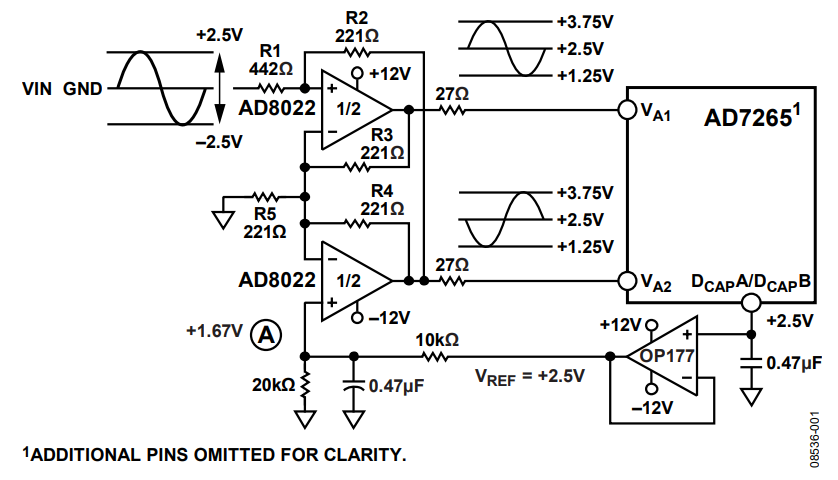
主负反馈路径由AD8022 R2至R1电阻构成,从AD8022 VIN输入信号到AD7265 VA2 引脚的增益由R2与R1的比值设置。本例中,该比值为0.5。AD8022上半部分输入端的1.67 V共模电压在 VA2 引脚产生输出共模电压,即(1 + R2/R1) × 1.67 V = 2.5 V。电阻R3和R4提供的局部反馈在 VA1处产生信号,该信号与 VA2处的信号180°错相。
输入电压为0 V时, VA1和VA2均必须为2.5 V。这要求R3和R4的电流均为(2.5 V–1.67 V)/221 Ω = 3.76 mA。因此,流过R5的电流为2 × 3.76 mA= 7.52 mA。所以,R5必须等于R3和R4,使 VA1处的共模电压必须为2.5 V。
AD7265可以总共有12个单端模拟输入通道。模拟输入范围可以通过编程设置为0 V至基准电压(VREF)或0 V至2 × VREF。图2所示为ADC以单端模式工作时的典型连接图,其中AD8022用于驱动两个单端输入。AD8021是一款高性能单通道运算放大器,在极高性能系统中可以替代双通道器件。电阻网络(R)的绝对值可以灵活选择,但是必须根据所要实现的运算放大器带宽来选择。

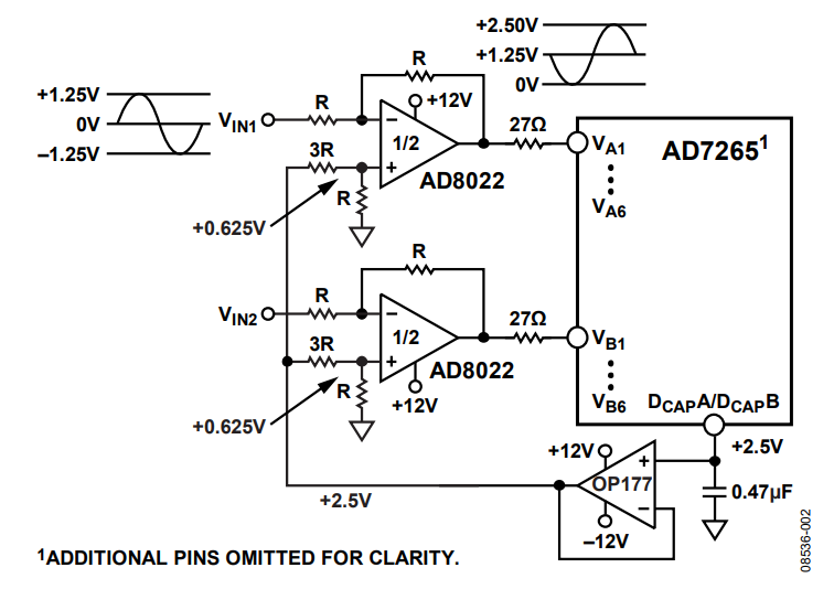
图1和图2中的AD8022均采用12 V双电源供电,而AD7265的额定电源电压范围为2.7 V至5.25 V。瞬态或上电情况下决不能超过AD7265的最大输入电压限制(请参考“教程MT 036”)。该电路还必须构建在具有大面积接地层的多层PCB上。为实现理想性能,必须采用适当的布局、接地和去耦技术(请参考教程MT-031、教程MT-101及EVAL-AD7265)。
常见变化
如需降低成本,可以使用超低失调电压运算放大器OP07D代替OP177。除失调电压(VOS)特性外,二者的性能相似。
参考电路
Walt Kester、James Bryant 和 Mike Byrne,教程 MT-031, 实现数据转换器的接地并解开AGND和DGND的谜团,ADI 公司。
教程 MT-036,运算放大器输出反相和输入过压保护,ADI公司。