AN-1479: ADuCM4050 SPI Flow Control Modes
Introduction
The serial peripheral interface (SPI) is an industry standard, synchronous serial link that allows full duplex operation to other SPI-compatible devices, which include analog-to-digital converters (ADCs), digital-to-analog converters (DACs), digital potentiometers, nonvolatile memories (NVMs), sensors, and microcontroller units (MCUs). Some of these devices have special features for specific purposes, such as achieving a high speed, event notification, and command response mechanisms.
The enhanced modes of operation of the ADuCM4050 SPI has provide the user the flexibility of half-duplex operation and flow control options, which automatically enable the SPI block to use most of these specific characteristics of the peripherals in hardware. Therefore, user code is simplified and energy efficiency can be improved.
This application note describes the SPI flow control modes available in the ADuCM4050 MCU and shows several examples of use.
Background
Flow control is necessary to synchronize the data flow between a master and a slave. The ADuCM4050 MCU provides flow control as a differentiating feature in the SPI. Along with read command mode, flow control can be used to receive multiple data bytes.
With flow control, the data transfer between the SPI master and slave is controlled based on the application requirements in terms of periodic data or demand-based data read.
The SPI master in the ADuCM4050 supports the following modes of flow control:
- Pin-based flow control, controlled by the SPI slave.
- Based on the MISO pin.
- Based on the RDY pin.
- Timer-based flow control, controlled by the SPI master.
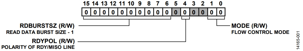
The flow control modes are described in the following sections in more detail. The mode field in the SPI flow control register (SPI_FLOW_CTL) configures the flow control mode to any one of the three modes. Figure 1 shows the SPI_FLOW_CTL register.
Note that flow control mechanisms can be used only when the ADuCM4050 is configured as an SPI master.
Pin-Based Flow Control
Using a Separate RDY Pin
Some SPI slaves have a dedicated RDY pin that is connected to the SPI_RDY pin of the SPI master, in this case, the ADuCM4050. The SPI_RDY pin is a dedicated pin (as an alternate functionality to a general-purpose input/output (GPIO)) for every SPI instance.
For example, the ON Semiconductor® CAT64LC40 serial flash uses a dedicated RDY pin to signal the availability of data to the SPI master.
The RDY pins of the ADuCM4050 can be wired to an interrupt pin of the SPI slave in case the slave does not support a dedicated RDY pin. The slave uses the RDY pin to indicate that the acquisition and data processing is complete. The master does not provide SPI clock until it sees an active level on this pin.
The user can configure the number of bytes to be read when the RDY pin is asserted. Perform this configuration by setting the RDBURSTSZ field in the SPI flow control register (SPI_FLOW_ CTL). After receiving this burst of bytes on MISO, the SPI master continues to wait for the next RDY pin assertion to receive the next set of bytes. This process is repeated until all bytes as set in the SPI count register (SPI_CNT) are received.
Note that when using read command mode, a maximum of 16 bytes can be transmitted. This transmission is configured using the TXBYTES field of the SPI read control register (SPI_RD_CTL). The number of bytes received in one burst when using flow control is set in the RDBURSTSZ field of the SPI flow control register (SPI_FLOW_CTL). However, the total number of bytes to be received does not have an imposed maximum limit.
Using the MISO Pin
Some SPI slaves do not have a dedicated RDY pin but have a provision to reuse the MISO pin to inform the SPI master that the data is ready to be sent on MISO. This is typical in some ADCs, like the AD7798.
The ADuCM4050 SPI master waits for an active level transition on the MISO line and, when this is detected, reads RDBURSTSZ + 1 number of bytes and then returns to a wait state until another active level is detected on MISO.
The polarity of the MISO/RDY pin can be configured using the RDYPOL field of the SPI flow control register (SPI_FLOW_CTL).
Timer-Based Flow Control
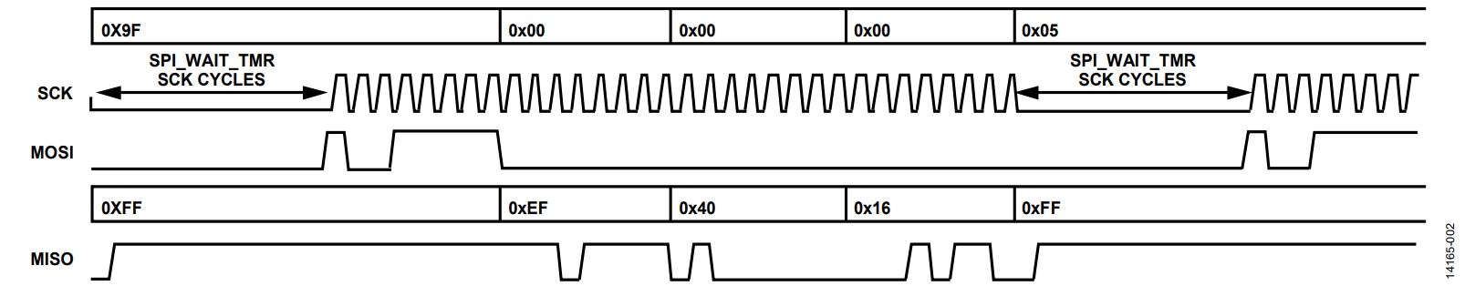
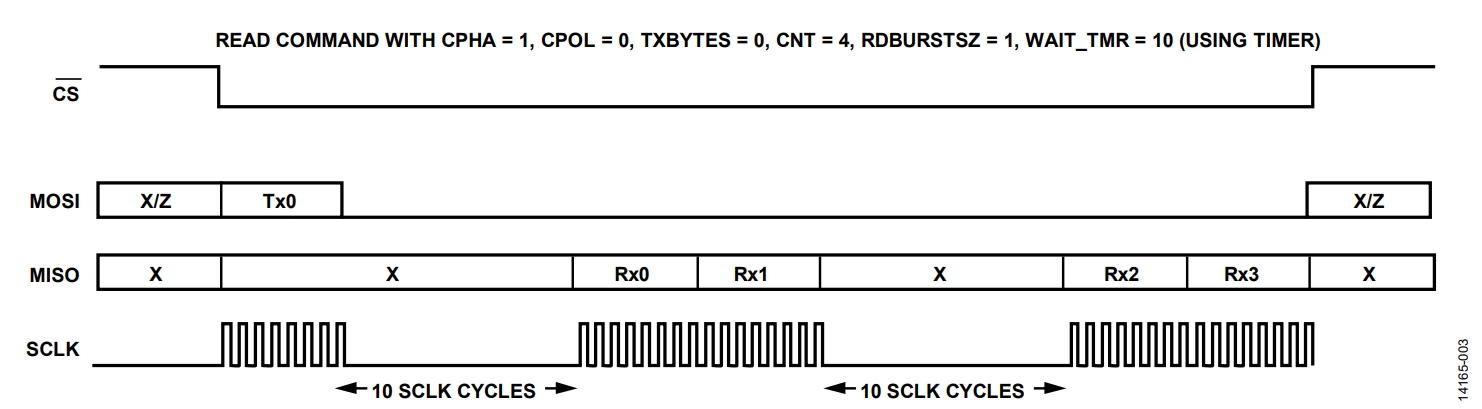
For slaves that do not have a dedicated pin to inform the availability of data to the master, the MCU uses a 16-bit timer to introduce wait states while reading data. When the timer triggers, the master reads a burst of bytes (RDBURSTSZ + 1) and then restarts the timer. The timer is clocked at the SPI clock rate (SCK), and the number of SCK cycles to wait before the timer is triggered can be set using the SPI_WAIT_TMR register. See Figure 2 for an example.
When this scheme is used to stall and drive SCK for flow control, ensure that the last SCK edge is a sampling edge. After the stall period is over, an SCK driving edge causes the next data transfer.


Source Code
This section uses the hardware flow control mode to demonstrate how the flow control feature can simplify the user code and power savings in a system.
This section contains two examples: one to show the timer-based concept, and another to show a pin-based example.
Timer-Based Flow Control Example
The first method to control a device automatically via SPI flow options is a timer. As discussed in the Timer-Based Flow Control section, the SPI block adds a configurable delay between successive transfers. This method is typical of some ADCs and sensors, which offer a data stream with a fixed frequency sampling and data rate.
The SPI flow method is indicated through the SPI_FLOW_CTL register. In this case, the timer option is set to 1 at the SPI_FLOW_ CTL.MODE bit field.
The delay depends on the PCLK frequency and the SPI_WAIT_ TMR register. The value of this registers specifies the number of SPI_CLK cycles (PCLK/SPI_DIV) to wait before a new SPI operation can be performed.
Other options to take into account are the following:
- SPI_CTL.CONTINUOUS bit field: the working sequence continues until all data are transferred.
- SPI_CNT register: the number of bytes to be transferred.
- SPI_FLOW_CTL.RDBURSTSZ bit field: the number of bytes to be read minus 1 per transfer.
The effect of those fields is shown in Figure 5.
In this example, the program reads a fixed number of words and, when it completes the task, the program finishes. The code is shown in the Code Sample 1 section.
Incoming data are read in the interrupt handler, where the read buffer is full and the values variable is increased (see the Code Sample 2 section).
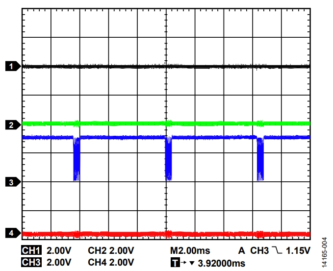
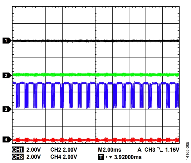
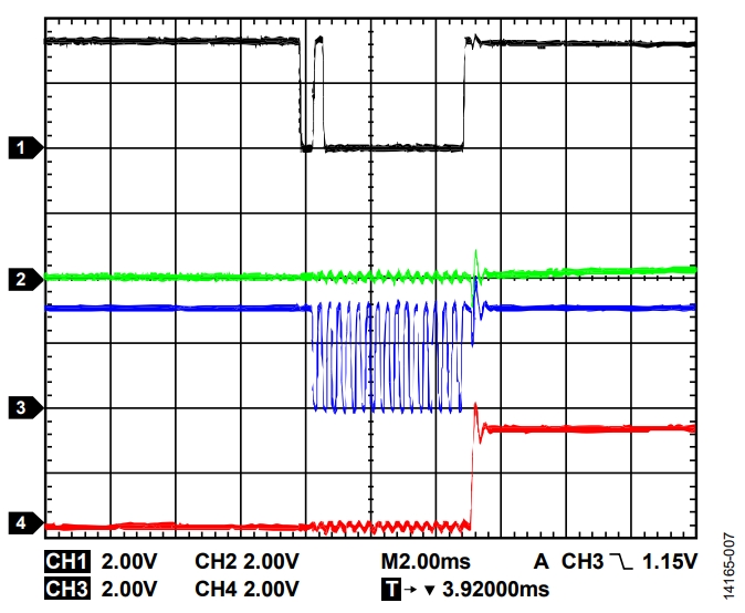
The result is shown in Figure 3 and Figure 4. These figures have been generated by changing the WAIT_TMR register value, which controls the delay between one burst and the next.


Code Sample 1
 #define NUM_VALUES 50
 volatile uint16_t values = 0;
 uint16_t buffer[NUM_VALUES] = {0};
[…]
 NVIC_EnableIRQ(SPI0_EVT_IRQn);


 pADI_SPI0->CS_OVERRIDE = 0;
 pADI_SPI0->CTL = (1 << BITP_SPI_CTL_CON) | //continuous
 (1 << BITP_SPI_CTL_CPOL) | //polarity
 (1 << BITP_SPI_CTL_CPHA) | //phase
 (1 << BITP_SPI_CTL_MASEN) | //master
 (1 << BITP_SPI_CTL_SPIEN); //enable
 pADI_SPI0->IEN = (1 << BITP_SPI_IEN_IRQMODE); //tx interrupt every 2 bytes
 pADI_SPI0->CNT = NUM_VALUES * 2; //bytes to be transferred (2 per sample)
 pADI_SPI0->RD_CTL = (0 << BITP_SPI_RD_CTL_TXBYTES) | //tx -1 for read command
 (1 << BITP_SPI_RD_CTL_CMDEN); //command mode
 pADI_SPI0->FLOW_CTL = (1 << BITP_SPI_FLOW_CTL_RDBURSTSZ) | //burst -1
 (1 << BITP_SPI_FLOW_CTL_MODE); //flow control based on WAIT_TMR
 pADI_SPI0->WAIT_TMR = 20; //number of cycles to wait


 tmp = pADI_SPI0->RX; //dummy read to initiate a Xfer


 while(values < NUM_VALUES); //wait for all the samples
Code Sample 2
 void SPI0_Int_Handler(){
   uint16_t aux = 0;


   if((pADI_SPI0->STAT & 0x20) == 0x20){ //TX done
     pADI_SPI0->STAT = 0x22;
   }else if((pADI_SPI0->STAT & 0x40) == 0x40){ //RX


     pADI_SPI0->STAT = 0xFFFF; // clear the interrupt


     aux = (pADI_SPI0->RX << 8);
     aux |= pADI_SPI0->RX;


     buffer[values++] = aux;
   }
 }
Pin-Based Flow Control Example
The second SPI flow method is the signaling of a new transfer. In this example, the MISO line is used as the ready signal.
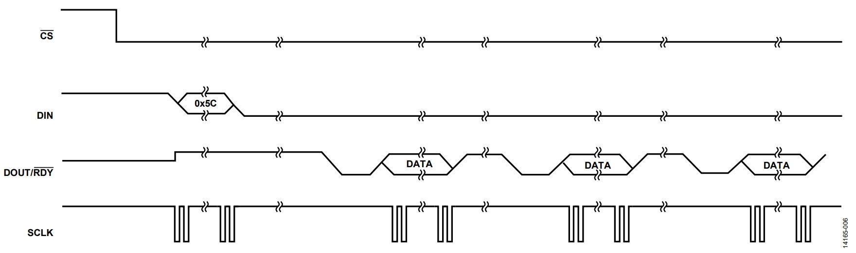
This example implements an interface to the AD7798 ADC. This ADC can be configured to work in an autonomous mode, which consists of sending samples automatically. The availability of a new sample is notified through the MISO line. Configuration to select the continuous mode is made by writing a value of 0x5C, which indicates in the COM register that the data register is the next one to be read in continuous mode.
Continuous mode is a means of continuously reading samples from the AD7798. Each sample is a 16-bit word available only after the MISO line is tied to ground by the ADC. The workflow is shown in Figure 7.
The ADuCM4050 SPI must be configured in MISO mode as the SPI flow option by writing a 3 in the SPI_FLOW_CTL.CTL_ MODE bit field. This method also takes into account the RDYPOL bit field in the same register. In this case a low value is the trigger, so a 1 must be written.
Because each transfer is a 16-bit width word, a 1 value is needed in SPI_CTL.IRQMODE, which is used to notify an interrupt when two bytes are available at the RX buffer. Furthermore, a 1 in SPI_FLOW_CTL.RDBUSTSZ indicates that 16-bit clock cycles are completed per transfer.
Finally, the configuration word (0x5C) must be written to the AD7798 to properly configure the device.
The code is shown in the Code Sample 3 section.
The reading can also be done in the interrupt handler function (see the Code Sample 4 section).
The result is a data stream, as shown in Figure 6. The AD7798 ADC signals that a new sample is available and puts this data on the MISO line (the yellow line). In each of the reads, the ADuCM4050 generates the clock (the blue line) and keeps the chip select line to low (the pink line) until the end of the entire transference. The MOSI line is not needed after the initial configuration (the green line).


Code Sample 3
 NVIC_EnableIRQ(SPI0_EVT_IRQn);


 pADI_SPI0->CS_OVERRIDE = 0;
 pADI_SPI0->CTL = (1 << BITP_SPI_CTL_CON) | //continuous
 (1 << BITP_SPI_CTL_CPOL) | //polarity
 (1 << BITP_SPI_CTL_CPHA) | //phase
 (1 << BITP_SPI_CTL_MASEN) | //master
 (1 << BITP_SPI_CTL_SPIEN); //enable
 pADI_SPI0->IEN = (1 << BITP_SPI_IEN_IRQMODE); //tx interrupt every 2 bytes
 pADI_SPI0->CNT = NUM_VALUES * 2; //bytes to be transferred
 pADI_SPI0->RD_CTL = (0 << BITP_SPI_RD_CTL_TXBYTES) | //tx -1 for read command
 (1 << BITP_SPI_RD_CTL_CMDEN); //command mode
 pADI_SPI0->FLOW_CTL = (1 << BITP_SPI_FLOW_CTL_RDBURSTSZ) | //burst -1
 (1 << BITP_SPI_FLOW_CTL_RDYPOL) | //ready signal polarization: LOW
 (3 << BITP_SPI_FLOW_CTL_MODE); //flow control based on MISO


 pADI_SPI0->TX = 0x5C; //configure AD7798 in continuous mode
 tmp = pADI_SPI0->RX; //dummy read to initiate a Xfer


 while(values < NUM_VALUES);
Code Sample 4
 void SPI0_Int_Handler(){
   uint16_t aux = 0;


   if((pADI_SPI0->STAT & 0x20) == 0x20){ //TX done
     pADI_SPI0->STAT = 0x22;
   }else if((pADI_SPI0->STAT & 0x40) == 0x40){ //RX


     pADI_SPI0->STAT = 0xFFFF; // clear the interrupt


     aux = (pADI_SPI0->RX << 8);
     aux |= pADI_SPI0->RX;


     buffer[values++] = aux;
   }
 }
Conclusion
The different features of the ADuCM4050 SPI, such as read command mode and flow control, make the device ideal for use in battery-powered systems where the SPI peripheral offloads the MCU and can be independently used for data collection.
Implementing these characteristics in hardware simplifies the user code because it is not required to program some actions, for example, delays or pulling a line. The characteristics of the ADuCM4050 provide efficient energy consumption because an MCU is not necessary.
The implementation of the characteristics of the ADuCM4050 in conjunction with the direct memory access (DMA) and flexi mode allow the user to drastically improve energy efficiency and productivity.