AN-1472: General Guidelines and Procedures for Using the HMC661LC4B and HMC1061LC5 with an ADC
Introduction
Wideband data acquisition systems with a multi GHz bandwidth are needed for a variety of applications, such as software defined radio, radar systems, electronic warfare (EW), electronic intelligence (ELINT), and test and measurement equipment. Ideally, system designers want to be able to connect the signal source (for example, an antenna) directly to a wideband, high dynamic range analog-to-digital converter (ADC) for digitization. Many of these applications involve subsampling where the signal of interest is a high frequency signal well beyond the ADC sample rate. A key limitation to this approach is that current ADCs do not usually have sufficient bandwidth for these very wideband applications. Although several high speed ADCs offer enhanced sample rates, few of them offer input bandwidth beyond a few GHz. In addition, maintenance of good sampling linearity at frequencies above the ultrahigh frequency (UHF) band is technologically challenging and most current ADCs suffer rapidly degrading linearity above a 1 GHz or 2 GHz signal frequency.
These limitations can be overcome using the HMC661LC4B or HMC1061LC5, ultra wideband track-and-hold amplifiers designed for use in microwave data conversion applications requiring maximum sampling bandwidth, high linearity over a wide bandwidth, and low noise. The HMC661LC4B, which offers an 18 GHz input bandwidth and excellent broadband linearity, is used as an external master sampler at the front end of the ADC. After extended bandwidth sampling takes place within the HMC661LC4B, the low bandwidth held output waveform can by processed by an ADC with substantially reduced bandwidth. The HMC1061LC5 is the dual rank version of the HMC661LC4B track and hold amplifier.
The ADC linearity limitations at high input frequencies are also mitigated because the settled track-and-hold amplifier waveform is processed with the optimal baseband linearity of the ADC. Additionally, the HMC661LC4B offers very low random sample jitter of <70 fs, which minimizes jitter induced signal to noise ratio (SNR) degradation at high microwave signal frequencies. This jitter is significantly better than that typically obtained from currently available ADCs. The result is a radical extension in input bandwidth, substantial improvement in high frequency linearity, and improved high frequency SNR for the track-andhold amplifier ADC assembly compared to the performance of the ADC alone.
This application note provides guidelines for using the HMC661LC4B with high speed ADCs to enhance their bandwidth and high frequency performance. An overview of track-and-hold amplifier operation and general operating recommendations for maximizing device performance are described in this application note. The setup and timing adjustment of a typical evaluation board-based breadboard assembly incorporating the HMC661LC4B as a master sampler for high speed ADCs is also provided. Examples of how the performance track-and-hold amplifier can be obtained when the HMC661LC4B is used in an evaluation board setup with high speed ADCs can be found in the Analog Dialogue article, Radically Extending Bandwidth to Crush the X-Band Frequencies Using a Track-and-Hold Sampling Amplifier and RF ADC.
HMC661LC4B Track-and-Hold Amplifier Description and Operation
HMC661LC4B Track-and-Hold Amplifier General Description
The HMC661LC4B is a single rank, 18 GHz, track-and-hold amplifier for use in microwave data conversion applications requiring maximum sampling bandwidth, high linearity over a very wide bandwidth, and low noise. A single track-and-hold amplifier produces an output consisting of two time segments. In the track mode interval of the output waveform (positive differential clock voltage for the HMC661LC4B), the HMC661LC4B behaves as a unity-gain amplifier, which replicates the input signal at the output, subject to the input bandwidth, and the output amplifier bandwidth limitations. At the positive to negative clock transition, the HMC661LC4B samples the input signal with a very narrow sampling time aperture and holds the output relatively constant during the negative clock interval at a value that is representative of the signal at the instant of sampling.
Refer to the HMC661LC4B data sheet for key performance parameters. Unlike other available high speed track-and-hold amplifiers, which suffer substantial bandwidth degradation at full-scale input levels, the HMC661LC4B provides an 18 GHz sampling bandwidth over the full range of input level up to a fullscale differential input of 1 V p-p and up to a 4 GSPS sampling rate. The track-and-hold amplifier maintains excellent linearity over a very broad bandwidth with 56 dB or better spurious-free dynamic range (SFDR) from dc to >5 GHz at the full-scale input. An important feature of the HMC661LC4B is that it exhibits proper linearity order dependence (a 6 dB reduction in input level results in 12 dB and 18 dB reduction in the second-order and third-order harmonic product levels, respectively). This feature is particularly important for designers who are employing signal averaging using digital signal processing (DSP). These users may perform post conversion processing to reduce the wideband noise floor and may choose to trade off input signal level for higher linearity. As the data sheet shows, a reduction of input level to half full-scale results in 10-bit or better linearity across a wide bandwidth.
The HMC661LC4B provides dc-coupled, differential signal inputs/ outputs, and differential clock inputs. All inputs and outputs are 50 Ω impedance for each differential half circuit and they operate at a true, ground referenced, common-mode voltage potential. The HMC661LC4B is housed in an RoHS-compliant, 4 mm × 4 mm, QFN, leadless ceramic package. The HMC661LC4B is ideal for software defined radio, military and commercial radar systems, EW, and ELINT systems applications. The HMC661LC4B can also be used for spread spectrum processing, wideband spectrum analysis, and high speed digital and analog test instruments, including digital sampling oscilloscopes.
HMC661LC4B General Operating Recommendations
Refer to the HMC661LC4B data sheet for complete details on operating conditions. Key operating notes are summarized in this application note for convenience of the reader.
Power Supply Sequencing
The recommended power supply start-up sequence is VCCOB, VCCOFx, VCCTHx, VCCCLKx, VEE, and VEECLKx, if biased from independent supplies. VCCOB, VCCOFx, VCCTHx, and VCCCLK can be connected to one 2 V supply if desired.
Input Signal Drive
For best results, the inputs must be driven differentially. The input can be driven single ended, but the linearity of the HMC661LC4B degrades. The unused input must be terminated in 50 Ω when driving the HMC661LC4B single ended.
Clock Inputs
The HMC661LC4B is in track mode when CLKP – CLKN is high and it is in hold mode when CLKP − CLKN is low. The clock inputs must be driven differentially if possible. The clock inputs can be driven single ended if desired, but the single-ended amplitude and slew rate must be similar to the full differential amplitude and slew rate recommended for differential drive. The unused input must be terminated to 50 Ω.
The track-and-hold mode linearity of the HMC661LC4B varies with clock power at lower clock frequencies, as shown in the HMC661LC4B data sheet. The linearity that varies with clock power results from a weak dependence of the linearity on the clock zero crossing slew rate for slew rates beneath a critical value. For optimal linearity and jitter, a clock zero crossing slew rate of roughly 2 V/ns to 4 V/ns (per clock input) or more is recommended.
For sinusoidal clock inputs, 4 V/ns corresponds to a sinusoidal clock power per differential half circuit input of −6 dBm at 4 GHz, 0 dBm at 2 GHz, and 6 dBm at 1 GHz. Regardless of the clock frequency, a minimum clock amplitude of −6 dBm is recommended (per differential half circuit input). At lower clock frequencies, particularly below 1 GHz, square wave clocks are suggested to achieve the desired slew rates without excessive clock amplitude.
Outputs
The outputs must be sensed differentially for the cleanest output waveforms. The output impedance is 50 Ω resistive returned to the VCCOB supply. The output stage is designed to drive 50 Ω terminated to ground on each differential half circuit output. The HMC661LC4B offers a true, ground referenced, commonmode voltage output that is typically within ±50 mV of ground; however, it is possible to adjust the VCCOB power supply slightly to fine tune the output common-mode voltage level to precisely 0 V if desired.
Additionally, the common-mode output level can be adjusted within the range of approximately ±0.5 V by adjusting the VCCOB power supply according to the following approximate relation:
VOCM = (VCCOB − 2)/2
where:
VOCM is the output common mode voltage.
VCCOB can be varied in the range of 1 V < VCCOB < 3 V
Users operating at lower clock rates (such as < 1 GHz) can optimize SNR by filtering the output to a lower bandwidth than the output amplifier bandwidth of 7 GHz. Such an output filter does not reduce the sampled front-end noise (which is captured in the signal samples and represents the majority of the track-and-hold amplifier noise because of the wide front-end bandwidth), but it can reduce the output amplifier noise contribution. The user can filter the output to the lowest bandwidth that still retains the maximum settling time required to support the chosen clock rate. Typically, optimal bandwidth is of the order of two to three times the clock rate. For example, a user operating at a clock rate of 350 MHz with a 1 GHz noise bandwidth output filter can achieve approximately 1 dB lower noise relative to the unfiltered output condition.
The output has very sharp transitions at the clock edges due to the broad output amplifier bandwidth. The user must be aware that any significant length of cable between the chip output and the load causes frequency response roll-off and dispersion, which can produce low amplitude tails with relatively long time constants in the settling of the output waveform into the load.
The load effect is most noticeable when operating in a lab setting with output cables of a few feet in length, even with a high quality cable. Output cables between the track-and-hold amplifier and the load must be of very high quality and of 2 feet or less in length.
Reflections between the load and the HMC661LC4B also degrades the hold mode response. The output cable length can be adjusted to minimize the reflection perturbations to some extent. In general, the round trip transit time of the cable must be an integer number of clock periods to obtain the minimal reflection perturbation in the hold mode portion of the waveform. This cable length criterion essentially approximates a scenario where the low level double transit reflections time align with the output waveform sourcing them. The optimal performance is obtained when the track-andhold amplifier is within 50 ps or less of the load because short distance and/or transit time gives a reflection duration equal to the approximate settling time of the HMC661LC4B. In ADC applications, the track-and-hold amplifier must be placed as close as possible to the ADC to minimize reflection effects on the path between the track-and-hold amplifier output and the input of the ADC.
Track-and-Hold ADC Setup and Timing
Track-and-Hold ADC Setup
A typical evaluation board laboratory setup using the HMC661LC4B as a master sampler for a high speed ADC is shown in Figure 1. Synthesized generators with very low jitter must be used for input and clock signals to minimize jitter induced noise floor degradation at high signal frequencies. Fractional bandwidth band-pass filters of 5% clean up the signal sources by filtering nonharmonic spurious products and broadband noise, which contribute jitter to the signal and clock sources. A broadband Picosecond Pulse Labs or equivalent phase splitter with 17 GHz bandwidth converts the single ended input signal to a differential format. The HMC-C004 wideband amplifiers are needed to amplify the signal and clock enough to compensate for the losses in the system.
If desired, more conventional lower frequency baluns can be used for the clock because the clock is limited to a much lower frequency. A variable delay line properly times the ADC clock so that the ADC samples the settled hold mode portion of the output waveform from the HMC661LC4B. DC blocking capacitors are used between the track-and-hold amplifier and the ADC for single-supply-based ADCs because the ADCs operate at a nonzero common-mode input voltage bias level, typically provided internally.
Alternatively, a dc-coupled differential amplifier with a variable output common-mode voltage level can be used to match the dc levels of the HMC661LC4B and the ADC. The HMC661LC4B has a 0 V nominal common-mode output level, but it can be adjusted over a ±0.5 V range if desired (see the HMC661LC4B data sheet for details).
As discussed previously, when using the HMC661LC4B in an actual system application, it is preferable to place the track-andhold amplifier in close proximity to the ADC to minimize the transit time of reflection effects on the signal interconnect between the devices. Placing the track-and-hold amplifier in close proximity to the ADC is best achieved by designing a custom board or hybrid that places the track-and-hold amplifier and the ADC next to each other. In this case, a fixed delay is designed into the ADC clock signal path to obtain the proper timing of the ADC clock with respect to the track-and-hold amplifier output waveform. However, as demonstrated in this application note, a breadboard type setup with coaxial cable interconnects provides accurate performance as long as the ADC clock is properly timed with respect to the track-and-hold amplifier clock.

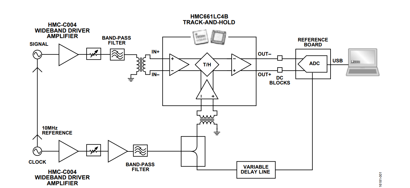
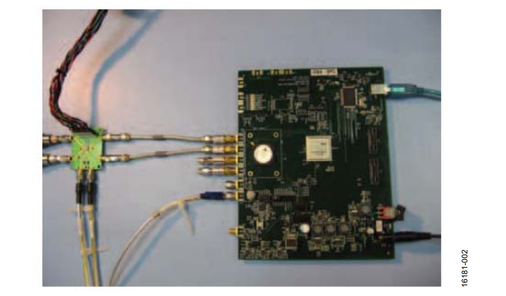
Figure 2 shows a photograph of the breadboard setup. The differential outputs of the track-and-hold amplifier evaluation board are connected to the dc blocks at the input of the ADC evaluation board via short Subminiature Version A (SMA) cables. At the two clock frequencies tested (1 GSPS and 1.6 GSPS) the cable length is chosen so that the total transit time from the trackand-hold amplifier chip to the ADC chip is approximately an integer number of clock cycles to minimize the waveform perturbations arising from the double transit reflection effects described previously.

Track-and-Hold ADC Timing
An important aspect of proper operation of the track-and-hold amplifier ADC conversion assembly is establishing the correct timing of the ADC sampling with respect to the track-and-hold amplifier output waveform. The timing of the ADC sampling with respect to the track-and-hold amplifier is referred to as the relative ADC clock delay. For proper operation, the ADC must sample the settled portion of the hold mode output time segment in the track-and-hold amplifier output waveform. Although the assembly functions when the ADC is improperly timed to sample the track-and-hold amplifier track mode output waveform segment, the proper bandwidth expansion is not obtained because the ADC is sampling a buffered (but not sampled) unity-gain version of the input signal. In fact, the primary indicator that the ADC is properly sampling the hold mode time segment is the extended bandwidth behavior. If the composite assembly shows a bandwidth more similar to the ADC input bandwidth, then in all likelihood the timing is not properly adjusted and the ADC is sampling the track mode portion of the track-and-hold amplifier output waveform.
The relative ADC clock delay can be calculated accurately if the various propagation delays of the board transmission lines interconnect and the external cables are tabulated in addition to the internal group delays of the key paths inside the track-and-hold amplifier and the ADC. Table 1 shows the two key HMC661LC4B internal group delays relevant to the detailed computation of proper ADC clock timing: clock to hold node delay and hold node to output sample delay.
The input signal to hold node delay shown in Table 1 is not a quantity that must be known for ADC clock timing calculations, but it is included here for information purposes. A key parameter also needed in this computation is the ADC aperture delay, defined as the difference between the clock delay to the ADC internal sample point and the signal delay to the ADC internal sample point. Aperture time, along with breadboard level interconnect delays, can often overshadow the small delays in the HMC661LC4B track-and-hold amplifier.
These calculations are typically worthwhile or even necessary for a system implementation (although system timing is usually easier than a breadboard setup since the interconnected delays are much smaller). If the proper ADC clock delay (with respect to the track-and-hold amplifier clock) is determined and implemented accurately, then the resulting assembly can be properly timed for all clock frequencies with only one ADC clock delay. If the proper delay is only implemented within a modulo clock period (for example, proper phasing within a clock period but not the minimum required delay), then the setting is valid only for the specific clock frequency used. However, the detailed calculation and design of the necessary ADC clock delay is usually not necessary for laboratory breadboard setups since there is a simple algorithmic approach that can be performed with a variable delay line in the ADC clock path to rapidly arrive at the proper delay as described in Table 1.
| Path | Group Delay (ps) |
| Signal Input to Hold Node | 41.5 |
| Clock Input to Hold Node | 35 |
| Output Buffer Delay from Hold Node to Output | 43 |
An algorithmic approach to a timing setup that uses a variable delay in the ADC clock path and the fast-Fourier transform (FFT) output display of the ADC can be established. Before describing the procedure, it is helpful to understand how some of the key ADC output performance parameters depend on sampling position within the external HMC661LC4B trackand-hold amplifier waveform. Figure 3 shows the delay mapping of signal amplitude, SFDR, and noise spectral density as a function of the relative delay of the ADC clock (ADC sample point) with respect to the track-and-hold amplifier clock for the HMC661LC4B and ADC combination. The data shown in Figure 3 is taken for a 1 GSPS sample rate. For reference, the approximate time locations of the HMC661LC4B output waveform track-tohold transition and the hold-to-track transition are also indicated. The HMC661LC4B hold mode is bound between these points while the track mode time segment falls outside of the region bound by these points. This set of curves becomes very useful for understanding delay setup when the input frequency to the assembly is chosen well outside the bandwidth of the ADC. In Figure 3, the curves are plotted for an input signal frequency of 5 GHz, which is well beyond the approximately 2.8 GHz bandwidth of the particular ADC.

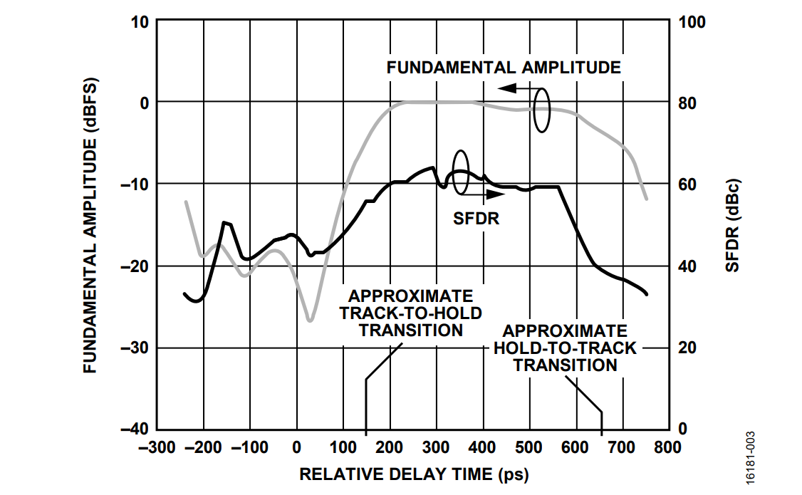
The waveform presented to the internal sampler of the ADC is band limited by the input signal bandwidth of the ADC. The band limiting within the ADC internal front end track-and-hold amplifier causes a substantial rounding of the curve of the sharp waveform transitions that are output from the HMC661LC4B. Therefore, the delay mapping curves shown in Figure 3 also exhibit rounded transitions due to this ADC band limiting. Using a first-order approximation, the −3 dB points of the amplitude curve correspond approximately to the time points of the trackto-hold and hold-to-track transitions of the HMC661LC4B output waveform.
From inspection of delay mapping curves similar to those shown in Figure 3 at a signal frequency beyond the ADC bandwidth but within the track-and-hold amplifier bandwidth, the key behaviors described in the Signal Fundamental Amplitude section, SFDR section, and the Noise section, can be deduced.
Signal Fundamental Amplitude
The bandwidth of the external track-and-hold amplifier is obtained when the ADC samples the hold mode of the track-and-hold amplifier waveform. The lesser bandwidth of the ADC is obtained when the ADC samples the track mode of the track-and-hold amplifier waveform. Samples in the transition regions can result in radical reductions in fundamental signal amplitude because the sample is not well defined at these points. The radical reduction effect can be observed in the fundamental amplitude variation of Figure 3 where the amplitude near the transition points decreases significantly. In the track mode region, the fundamental amplitude equilibrates at a constant level representative of the signal attenuation produced by the ADC input transfer function at that frequency.
SFDR
SFDR is relatively constant for ADC samples within the majority of the hold mode region of the track-and-hold amplifier waveform. It is preferable to ensure that the samples are taken near the end of the hold mode where the waveform is well settled, but before the hold-to-track transition rounding region caused by the ADC band limiting. As the clock frequency increases, it becomes more important to optimize the position of the samples in the hold mode time segment to achieve maximum SFDR. For the ADC measured, a reasonable ADC sampling time is about 120 ps advanced (earlier in time) with respect to the hold-totrack transition point. SFDR decreases rapidly when the ADC sample point enters the hold-to-track transition region because the signal sample is not well defined at these transition points.
Noise
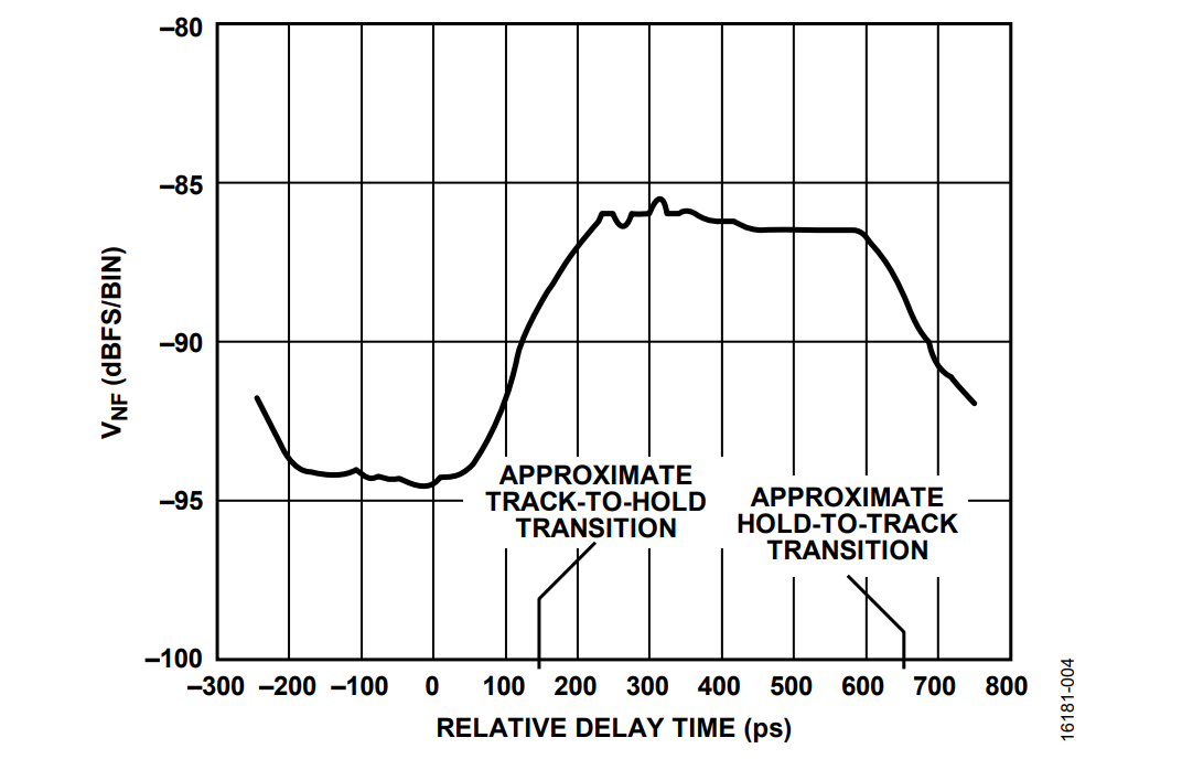
Figure 4 shows that the noise spectral density increases when the ADC samples are taken in the hold mode waveform segment relative to those taken in the track mode segment.
The noise spectral density increase can also be observed in the total integrated time domain noise as well. The increase is expected theoretically and it occurs because ADC samples in the hold mode region reflect the sampling of the HMC661LC4B over the full 18 GHz input bandwidth. From a frequency domain standpoint, the sampling process folds the noise over this entire bandwidth into the much lower bandwidth of one Nyquist interval. From a time domain standpoint, this effect can be viewed as the instantaneous front-end noise being effectively captured in the samples at the instant of sampling; this increases the noise spectral density in the first Nyquist interval, which is fully detected by the ADC because it falls within its input bandwidth. On the other hand, samples in the track mode region do not reflect sampling by the HMC661LC4B. The noise spectrum still occurs over 18 GHz of bandwidth, but the ADC never comprehends the HMC661LC4B sampling, and there is no folding effect for the ADC samples in the track mode portion of the waveform. The majority of this spectral noise falls outside of the bandwidth of the ADC, reducing the total noise detected.
The input noise bandwidth is 18 GHz for ADC samples in the hold mode region of the HMC661LC4B output waveform, while the input noise bandwidth is the ADC input bandwidth for ADC samples in the track mode of the HMC661LC4B. For example, it is not unusual to observe an 8 dB to 10 dB difference between the noise levels of the hold mode and track mode ADC samples for the 2 GHz to 3 GHz input bandwidths of typical high speed converters. This difference is expected because the ratio of the bandwidths is also approximately 8 dB to 10 dB, which makes the relative noise level a useful parameter to indicate the timing region of the ADC samples.

Simple Track-and-Hold ADC Timing Procedure for Breadboard Setups
While using the characteristics described in the Signal Fundamental Amplitude section and SFDR section, a straightforward approach can be established for determining the ADC clock timing and optimization in a typical breadboard setup. The following procedure uses a variable delay in the ADC clock path and the information provided by the FFT spectrum of the ADC:
- Set up the track-and-hold amplifier ADC timing with an arbitrary ADC clock delay and a variable delay. Set up the track-and-hold amplifier ADC timing initially with an arbitrary ADC clock delay (no need for detailed calculations) and a variable delay, with respect to the track-and-hold amplifier clock. The variable delay must allow adjustment over at least half of a clock cycle. Place the initial position of the delay in the center of the delay range. Due to the fixed pedestal delay of most trombone type variable delay lines, it can be helpful to use identical variable delays in both the track-and-hold amplifier clock and the ADC clock paths so that the fixed pedestal delay is balanced in both paths. Using identical variable delays is extremely helpful when setting the exact ADC clock delay for clock frequency independent timing where no excess modulo clock period delay can be tolerated. The relative ADC delay can then be adjusted by either or both of the delay lines. Balanced length cables must be used in the HMC661LC4B clock path between the balun and the clock inputs if the clock is driven differentially.
- Apply an input signal near full-scale outside the bandwidth of the ADC but within the bandwidth of the track-and-hold amplifier. Apply an input signal at a level just beneath ADC full-scale, at a frequency that is well beyond the ADC input bandwidth but within the HMC661LC4B track-and-hold amplifier bandwidth. A frequency of 5 GHz is a good choice for converters with 2 GHz to 3 GHz input bandwidth.
- Observe the FFT spectrum and identify the first order beat product (fundamental). Power up the ADC and HMC661LC4B devices; observing a FFT spectrum display of the ADC output and identify the first order beat product resulting from heterodyning the input signal with the clock harmonic track-and-hold amplifier places the resultant beat product in the first Nyquist interval. The beat product is the fundamental of interest, which is representative of the converted signal amplitude. For example, for a clock frequency of 1 GHz and an input signal frequency of 5.049 GHz, the downconverted first order beat product is at 5.049 − 5(1) = 49 MHz.
- Determine whether the ADC sample is occurring in the track mode or the hold mode region of the external track-and-hold amplifier output waveform. The determination of whether the ADC sample is occurring in the track mode or the hold mode region is accomplished by observing the fundamental amplitude. If a signal close to full-scale is obtained, then the ADC clock timing is sampling the hold mode waveform segment and the assembly is exhibiting the expanded bandwidth of the HMC661LC4B. If the signal amplitude observed is representative of the transfer function attenuation obtained from the ADC input bandwidth at that frequency, then the ADC is sampling the track mode waveform segment and exhibiting the reduced bandwidth of the ADC. If there is uncertainty in the status of the fundamental amplitude, then mapping the amplitude and noise of a few different delay points initially over a small delay range (such as ±50 ps) can rapidly assess if the ADC sample point is located on a track-to-hold or hold-to-track transition. If the sample point is located on a transition point, then shift the delay to avoid the transition region so that the samples land squarely in either the track mode or hold mode regions. In addition, mapping a few amplitude and noise points spread over a half clock cycle can rapidly assist in determining the operating regime and the location of transitions.
- Set the track-and-hold amplifier clock polarity to place the ADC samples in the hold mode of the HMC661LC4B. If the ADC is sampling the hold mode in Step 4, then the phasing of the track-and-hold amplifier clock connections can be left alone. If the ADC is sampling the track mode, then the differential clock connections to the track-and-hold amplifier must be reversed to shift the relative sampling delay between the track-and-hold amplifier and ADC by one half clock cycle. The differential clock connection change places the ADC sample point in the hold mode waveform segment. If the amplitude does not increase to near full-scale after shifting the clock phase to the track-andhold amplifier, then vary the ADC clock delay by small amounts while monitoring to assess if the ADC samples happen to be located on a transition point.
- Identify the hold-to-track transition and set the ADC sample point halfway between the track-to-hold and hold-to-track window of time with respect to this point. After the ADC samples are known to be in the hold mode, map a few points with increasing ADC clock delay until the location of the hold-to-track transition is determined. To first order, the hold-to-track transition occurs at about the −3 dB point of the delay mapping amplitude curve. Once the hold-to-track transition is identified, the ADC sample point can be advanced in time with respect to this transition until the amplitude and SFDR performance reach relatively equilibrated values. This location in time that achieves the expected amplitude and SFDR values occurs 30 ps to 150 ps advanced with respect to the hold-to-track transition, depending on the input bandwidth of the ADC and the resulting amount of band limiting rounding of the transition. The location in time point represents an acceptable point for the ADC sample timing. If the ADC relative delay has been set to the absolute minimum (no excess modulo clock period delay), then the timing is valid for all clock frequencies. If the ADC relative delay has only been properly phased but contains excess modulo clock period delay, then the timing procedure must be redone if the clock frequency changes.
Conclusion
This application note discusses the HMC661LC4B ultra wideband track-and-hold amplifier and its application as a master sampler for bandwidth and linearity enhancement in high speed ADCs. Guidelines for interfacing the HMC661LC4B to ADCs are presented and a simple systematic approach for establishing proper ADC sample time via clock timing in a breadboard setup is provided.
The Analog Dialogue article, Radically Extending Bandwidth to Crush the X-Band Frequencies Using a Track-and-Hold Sampling Amplifier and RF ADC, provides examples of the performance that can be obtained when the HMC661LC4B is used in an evaluation board setup with high speed ADCs.