AN-1408: 利用AD8376 VGA驱动高中频交流耦合应用中的宽带宽ADC
电路功能与优势
本应用笔记所述电路采用双通道、数字控制、可编程、超低失真、高输出线性度、可变增益放大器(VGA) AD8376和高速模数转换器(ADC),可实现高性能、高频采样。AD8376针对高频中频(IF)采样ADC驱动进行了优化。与ADI公司的高速ADC(如AD9445或AD9246)配合使用时,在100 MSPS以上、最大增益条件下,它可提供出色的无杂散动态范围(SFDR)性能。

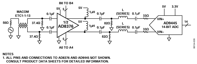
图1. 采用AD8376和AD9445的宽带ADC接口示例
电路描述
该电路采用AD8376 VGA,能够为AD9445等高速ADC提供可变增益、隔离和源阻抗匹配。利用该电路,当AD8376的增益为20 dB(最大增益)时,在100 MHz时的SFDR性能可达到86 dBc,如图2所示。

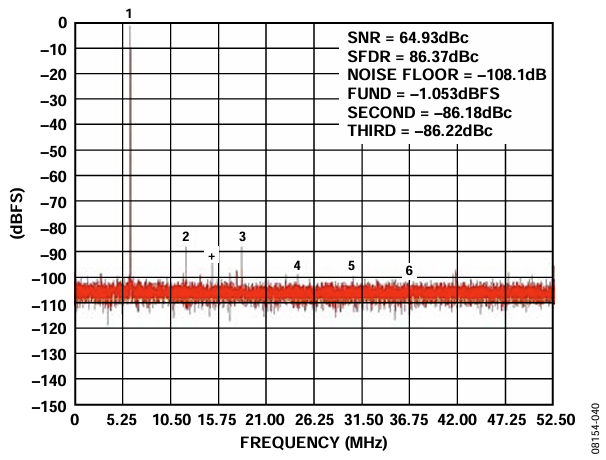
图2. 图1所示电路在100 MHz输入信号、105 MSPS采样速率时测得的单音性能
AD8376 VGA由宽带1:1传输线巴伦(或阻抗变压器)以差分方式驱动(以实现最佳性能),巴伦后接与AD8376的150 Ω输入阻抗并联的两个37.4 Ω电阻。这样可实现与50 Ω源的宽带匹配,如图1所示。AD8376的集电极开路输出通过两个1 μH电感偏置,并交流耦合至两个82 Ω负载电阻。82 Ω负载电阻与串联端接ADC阻抗并联,一同实现150 Ω目标差分负载阻抗,这是获得AD8376额定增益精度的建议值。负载电阻通过AD9445交流耦合,以消除共模直流负载。33 Ω串联电阻有助于改善AD8376与模数采样保持输入电路所有开关电流之间的隔离。
在可用的24 dB增益范围内,AD8376的输出三阶交调截点(IP3)和本底噪声基本上保持不变。对于接收机增益改变时需保持恒定瞬时动态范围的可变增益接收机而言,这一特性很重要。输出噪声密度的典型值约为20 nV/√Hz,与14位至16位灵敏度极限相当。AD8376的双音IP3性能典型值约为50 dBm。因此,驱动14位、105 MSPS/125 MSPS模数转换器AD9445时,在输入频率最高达140 MHz的条件下,SFDR性能优于86 dBc。使用AD8376时,有多种配置方式可供设计人员选择。集电极开路输出能够驱动多种不同负载。图1显示了一个简化的宽带接口,其中AD8376驱动AD9445。AD9445为14位、125 MSPS模数转换器,具有缓冲宽带输入,由此产生2 kΩ||3 pF差分负载阻抗,要求具有2 V峰峰值差分输入摆幅才能达到满量程。在图1中,加入串联电感L(串联)可扩展系统的带宽,并实现平坦的响应。当L(串联)为100 nH电感时,便可获得图3所示的宽带系统响应。在预失真接收器设计和仪器仪表等宽带应用中,宽带频率响应也是一个优势。但是,若针对较宽的模拟输入频率范围进行设计,由于高频噪声会混叠至目标奈奎斯特频率区域,因此级联信噪比(SNR)性能会有所下降。

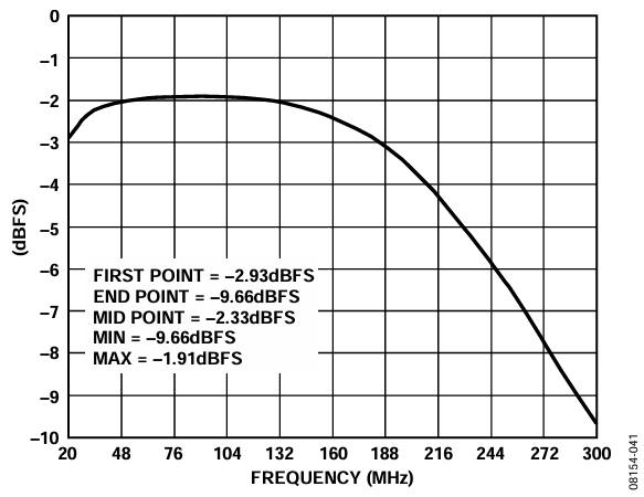
图3. 图1所示宽带电路的频率响应测量结果
常见变化
图4提供了另一种窄带方法。通过在AD8376与目标ADC之间设计一个窄带通抗混叠滤波器,目标奈奎斯特频率区域外的AD8376输出噪声得以衰减,有助于保持ADC的可用SNR性能。

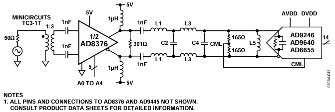
图4. 无缓冲开关电容ADC输入的窄带IF采样解决方案
一般而言,若用一个恰当阶数的抗混叠滤波器,SNR性能会提高数个dB。例如,采用一个低损耗1:3(阻抗比)输入变压器,使AD8376的平衡输入(150 Ω)与非平衡源(50 Ω)相匹配,从而使输入端的插入损耗最小。
图4所示窄带电路针对ADI的一些颇受欢迎的无缓冲输入 ADC驱动进行了优化,如AD9246、AD9640和AD6655等。表1列出了针对常用的IF采样中心频率,相关抗混叠滤波器元件的推荐值。电感L5与片内ADC输入电容及C4所提供电容的一部分并联,构成一个谐振电路。该谐振电路有助于确保ADC输入在目标中心频率条件下像个真实的电阻。此外,在直流时电感L5会使ADC输入短路,从而将一个零点引入传递函数。1 nF交流耦合电容和1 μH偏置扼流圈会将更多零点引入传递函数。最终的整体频率响应呈现出带通特性,有助于抑制目标奈奎斯特频率区域外的噪声。表1提供了一些初步建议值供原型设计使用。可能还需要考虑一些经验优化方法,帮助补偿实际的印刷电路板(PCB)寄生效应。关于级间滤波器设计的详细信息,参见“参考文献”部分。
针对图1中电路的两个37.4 Ω值(1/10 W),要求使用1%电阻。其他电阻的精度可以为10% (1/10 W)。电容须为10%陶瓷芯片电容。针对图4中电路的两个165 Ω值(1/10 W),要求使用1%电阻。其他电阻、电容和电感的精度可以为10%。
为使本应用笔记所讨论的电路达到理想的性能,必须采用良好的布局、接地和去耦技术。至少须采用四层PCB:一层为接地层,一层为电源层,另两层为信号层。
所有IC电源引脚都必须采用0.01μF至0.1 μF(为简易起见,未在图中显示)的低阻抗多层陶瓷电容(MLCC),去耦至接地层。还应遵循AD8376、AD9246和AD9445等器件的数据手册中的相关建议。
有关布局布线和关键元件定位的建议,请参考AD8376、AD9246和AD9445产品评估板。可以通过器件的产品主页查询评估板。
为了防止损坏AD8376的内部静电放电(ESD)保护二极管,A0至A4和B0至B4数字输入、ENBA和ENBB不得比AD8376电源电压高出0.6 V以上,也不得比地电压低0.6 V以上。如果驱动AD8376的逻辑电源从AD8376的供电电源获得,则不会发生损坏。AD8376采用双极性工艺制造,不易闩锁。
即使AD8376和AD9445(或其他ADC)采用不同电源供电,因为ADC的输入信号为交流耦合信号,所以时序控制也不是问题。
关于AVDD和DVDD电源的正确时序(如果使用独立的电源),须参考相应的ADC数据手册。
| 中心频率(MHz) | 1 dB带宽(MHz) | L1 (nH) | C2 (pF) | L3 (nH) | C4 (pF) | L5 (nH) |
| 96 | 27 | 390 | 5.6 | 390 | 22 | 100 |
| 140 | 30 | 330 | 3.3 | 330 | 20 | 56 |
| 170 | 32 | 270 | 2.7 | 270 | 20 | 39 |
| 211 | 32 | 220 | 2.2 | 220 | 18 | 27 |
参考文献
Walt Kester,《高速系统应用》,第 2章(优化数据转换器接口),ADI公司。2006年。
Walt Kester, 《数据转换手册》,第 6和第7章,ADI公司。2005 年。
Walt Kester、James Bryant 和 Mike Byrne,教程 MT-031, 实现数据转换器的接地并解开AGND和DGND的谜团,ADI 公司。
教程 MT-036,运算放大器输出反相和输入过压保护,ADI公司。
Eric Newman 和 Rob Reeder,应用笔记 AN-827, 放大器与开关电容ADC接口的谐振匹配方法,ADI公司。