AN-1286: ADuCM350模拟前端在高噪声数字环境中的精度
引言
ADuCM350是一款完整、纽扣电池供电、高精密的片上计量仪,适合便携式设备应用,例如护理点诊断和穿戴式生命体征等监测设备。
ADuCM350模拟前端(AFE)集成了如下元件:16位、精密、160 kSPS ADC;0.2%精密基准电压源;12位、无失码DAC;以及可重新配置的超低泄漏开关矩阵。ADuCM350还内置一个基于Cortex™-M3的处理器、存储器和所有I/O连接,因而可支持带显示器、USB通信和有源传感器的便携式计量仪。ADuCM350采用120引脚8 mm × 8 mm CSP_BGA封装,额定工作温度范围为-40°C至+85°C。
ADuCM350专门针对电化学反应的高精度分析而设计。
本应用笔记介绍了ADuCM350模拟前端在四种高强度数字噪声环境下的稳健表现。

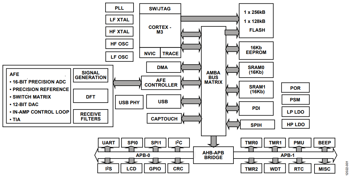
时序控制器/AFE控制器
ADuCM350利用自主时序控制器来控制模拟前端。因此,AFE能够以异步的方式对Cortex-M3处理器执行周期精确的操作。时序控制器可处理精密且时序关键的操作,而不受系统负载的影响。
Cortex-M3处理器使用RunSequence命令运行序列任务。它有两个独立的DMA通道,用于与时序控制器进行数据传输。为了保证操作完整性,它有两种故障安全操作:序列计数器,用于统计时序控制器执行的命令数量;CRC-8,应用于所有执行的命令。序列一旦开始,就会独立于核心运行,只能利用特定命令中止。
这一功能特性使得ADuCM350能够在高噪声数字环境中执行高精度且稳健的测量。

数字滤波
此模块实现了一个低通电源抑制滤波器,输出数据速率为900 SPS。要求是在直流电流测量阶段抑制50 Hz/60 Hz干扰。
滤波器模块由两个级联的sinc2滤波器组成。第一个滤波器(sinc2hf)将输入数据(以160 kHz采样的ADC数据)抽取至约900 Hz。第二个滤波器(sinc2lf)在50 Hz和60 Hz处添加陷波滤波器以抑制电源干扰。通常,滤波后的数据(sinc2lf)被提供给Cortex-M3,但也可以选择直接读取未经滤波的数据(sinc2hf输出)。
滤波器的建立时间为1/50 + 1/60 = 36.667 ms。
相关框图如图3所示。

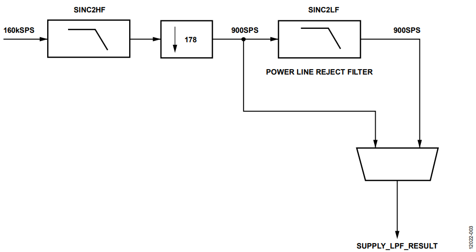
sinc2hf滤波器对160 kSPS输入数据进行1/178抽取,产生900 Hz的目标输出数据速率。选择900 Hz的原因是为了更好地对50 Hz和60 Hz进行陷波。
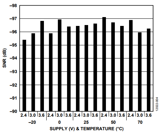
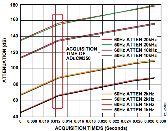
凭借这种配置带来的良好选择性,它非常适合在高噪声数字环境中稳健地进行高精度测量。TIA测量通道的信噪比曲线参见图4。

离散傅里叶变换模块
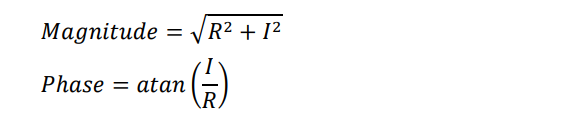
此模块执行2048点单频离散傅里叶变换(DFT)。它获取16位ADC的输出作为输入,输出复数结果的实部和虚部。
DFT引擎计算单个频点的信号功率,该频点是与激励频率相对应的频点。因此,正弦波形发生器和DFT引擎之间存在紧密耦合。DFT引擎使用频率控制字(AFE_WG_FCW)确定所需的频点。
DFT引擎输出复数结果。Cortex-M3通过下式计算激励频率下的阻抗幅度和相位:
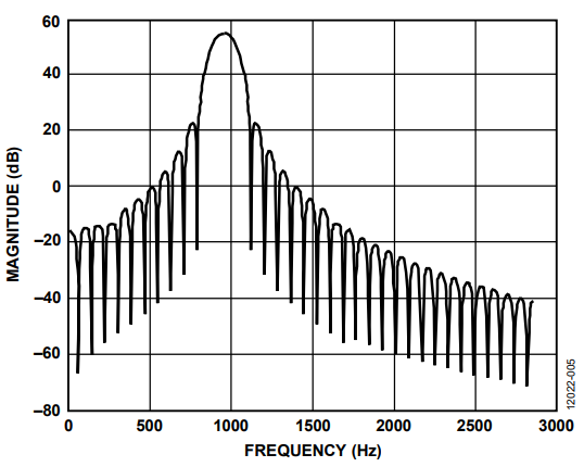
DFT函数经过优化,具有高度选择性和超窄带通滤波器性能,因此具备出色的抗噪声能力。有关对DFT性能进行的仿真,参见图6。


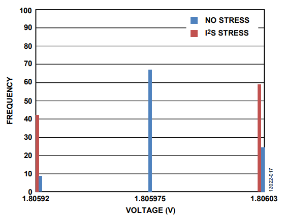
数字应力测试
本节介绍的测量旨在评估可能干扰精密模拟测量的数字噪声。ADuCM350上有许多数字模块,不能产生大量数字噪声,如UART、RTC和定时器。这些测试兼具实用性和针对性。
由于DFT具有较高的选择性,因此这些测量采用使能了Sinc2LPF的抽取ADC。
对于每项测试,第一组测量的条件是仅有ADC转换,而不施加应力。第二组测量的条件是使用时序控制器进行ADC转换,同时激励数字噪声源。
测量是在环境温度下进行的。
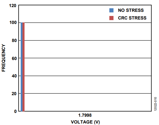
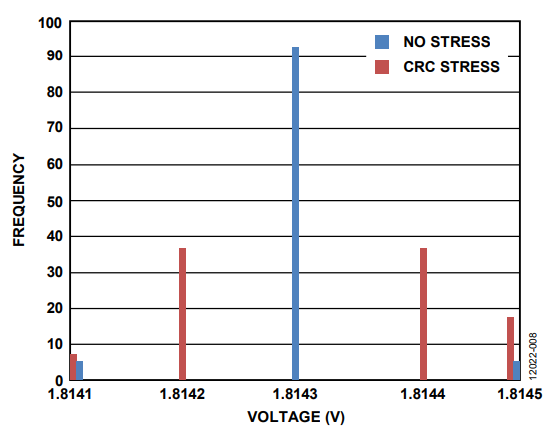
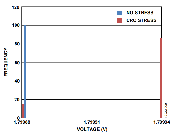
CRC应力测试
目的
数据传输测试:DMA执行512个从SRAM0(源)到CRC(目标)的32位传输,无等待状态。使用SRAM1重复此传输。此测试在利用AFE时序控制器进行精密模拟测量时循环进行。
测试的数字模块
- CRC
- DMA
- 总线矩阵
- SRAM0
- SRAM1
结果
结果表明,CRC应力噪声对模拟精度测量的影响可忽略不计。


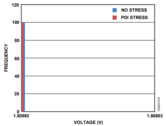
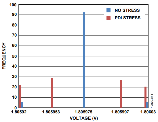
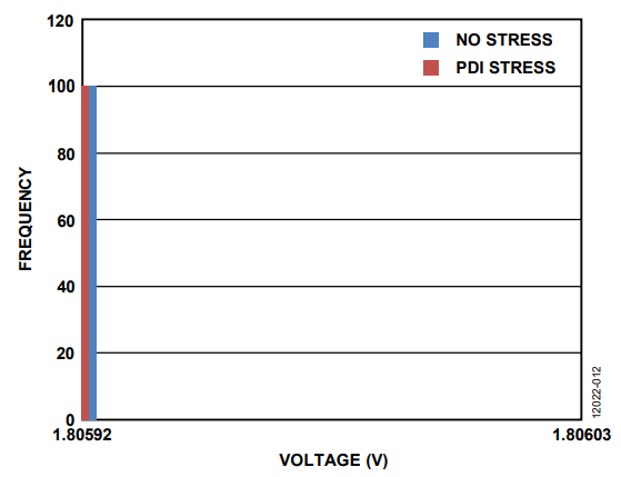
并行显示接口应力测试
目的
并行显示接口(PDI)与CRC类似,可在内部传输大量32位数据。此外,PDI还会切换宽并行端口(16位),在基本显示操作期间有可能会产生噪声。PDI代表单个接口可同时切换的最大引脚数。
数据在通用(GP)闪存中准备,并用作DMA源。数据通过DMA从GP闪存(源)传输到PDI(目标)。此测试以可能的最大数据速率运行。在进行精密AFE测量时,此传输会循环进行。
测试的数字模块
- PDI
- DMA
- 总线矩阵
- 通用闪存
结果
结果表明,PDI应力噪声对模拟精度测量的影响可忽略不计。


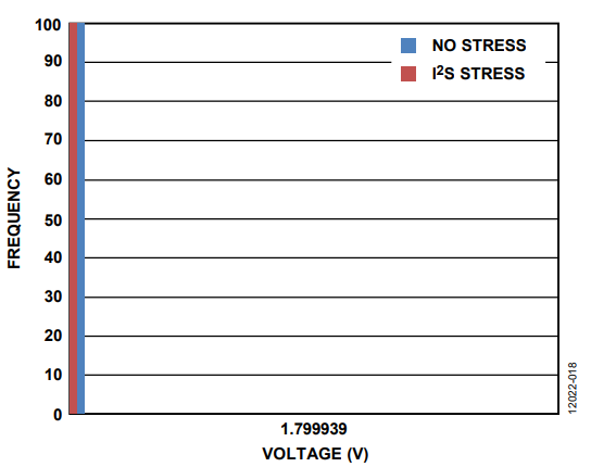
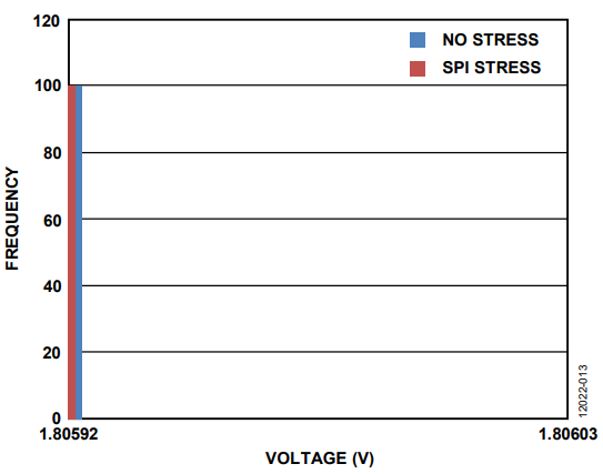
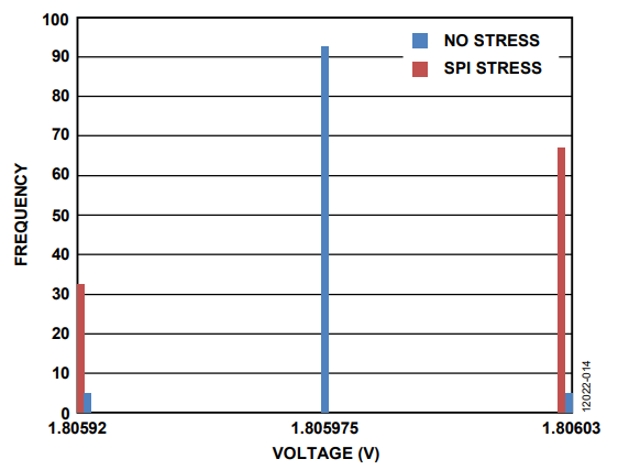
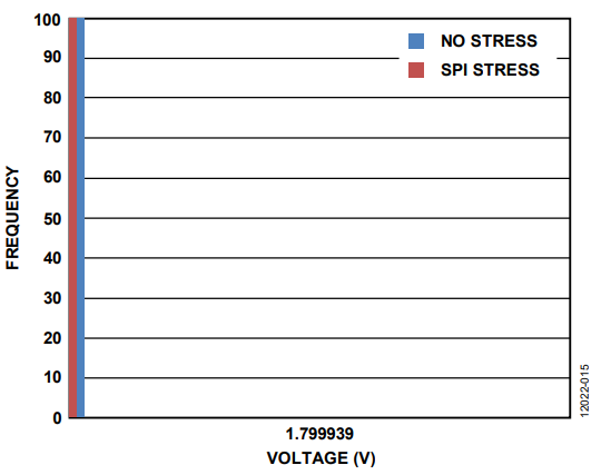
串行外设接口应力测试
高速SPI总线(SPIH)适合视频或音频数据的闪存存储。它支持8 MHz访问速度,并以突发方式运行。
在此应力测试中,SPIH设置为以8 MHz SCLK速度与SRAM 1进行512字节数据块的传输。DMA用于与SPIH进行数据传输。
测试的数字模块
- SPIH
- DMA
- 总线矩阵
结果
结果表明,SPI应力噪声对模拟精度测量的影响可忽略不计。


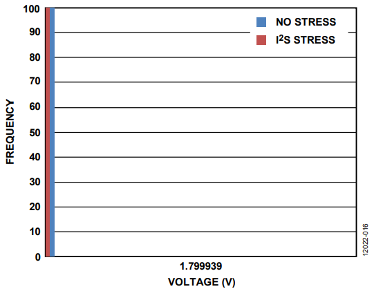
I2S 应力测试
I2S 代表以低性能音频速率通过系统连续进行8kbps数据速 率传输。这代表8 kHz采样速率、单声道,每个样本8位。它是使用DMA、SRAM、I2S和I/O引脚的稳定数据流的组合。
测试的数字模块
- I2S
- DMA
- SRAM1
结果
结果表明,I2S应力噪声对模拟精度测量的影响可忽略不计。