AN-1281: Amperometric/Potentiostat Measurements Using the ADuCM350
Introduction
The ADuCM350 is an ultra low power, integrated, mixed-signal metering solution that includes a microcontroller subsystem for processing, control, and connectivity. The processor subsystem is based on a low power Arm® Cortex®-M3 processor, a collection of digital peripherals, embedded SRAM and flash memory, and an analog subsystem, which provides clocking, reset, and power management capability.
The ADuCM350 is specifically designed for high precision analysis of electrochemical reactions.
This application note details how to set up the ADuCM350 to perform amperometric/potentiostat measurements on a resistor-capacitor (RC) sensor, which models a typical electrochemical cell.
Analog Front End (AFE) and Basic Loop TheoryDetails
AFE
The ADuCM350 AFE data acquisition loop consists of an excitation buffer amplifier loop, transimpedance amplifier (TIA), and switch matrix. The switch matrix is a programmable interface with an external sensor configuration and a calibration resistor.
The excitation buffer amplifier loop serves the following functions:
- Sources necessary sensor excitation current by buffering the filtered digital-to-analog converter (DAC) voltage.
- Provides gain to the AFE excitation loop to accurately set the sensor excitation voltage.
- Provides feedback capacitors and resistors in conjunction with the gain from the excitation buffer and places a zero in the loop to increase the gain excitation frequencies.
- Provides high impedance inputs for accurate sensing of excitation voltage through sense access resistance of the sensor.
The TIA serves the following functions:
- Provides current to voltage conversion for measurement by the analog-to-digital converter (ADC). The gain of the ADC is set by an external resistor.
- Sinks sensor excitation current.
- Ensures accurate setting of the working electrode voltage, which is the common mode for the sensor.
- Offers antialiasing filtering preceding the ADC.
The switch matrix serves the following functions:
- Allows calibration of unknown sensor impedance vs. an external known resistor.
- Allows measurement of sensor access resistances, switch resistances, and leakages for calibration.
Basic Loop Theory
Figure 1 shows a 4-wire sensor configuration. The stimulus voltage from the DAC is conditioned and buffered to the D node. This signal is switched through AFE8 (Switch D8 is closed) to the counter electrode of the sensor. The working electrode is held at a fixed common-mode voltage at AFE1 (Switch T1 is closed). This results in a current flow from the D node through the sensor to the T node. This current is converted to a voltage using the RTIA on the feedback path of the TIA.
Current into T Node = (VCOUNTER - VWORKING)/ZSENSOR
Voltage seen at ADC = Current into T Node × RTIAA
where:
VCOUNTER and VWORKING are voltages at opposite ends of the ZSENSOR.
ZSENSOR is resistance being measured.
RTIA is the gain resistor for the TIA.
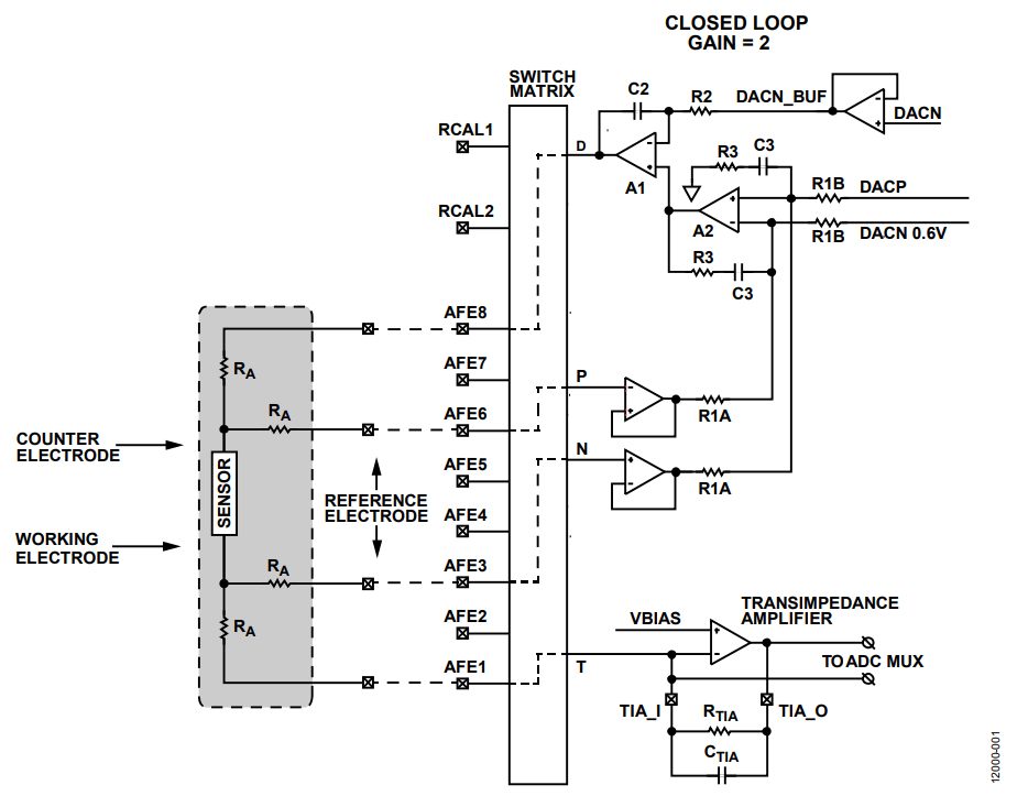
Figure 1. AFE Excitation Loop Block Diagram, 4-Wire Configuration.
The sensor is also sensed differentially by the P and N nodes. These nodes are fed back into the feedback loop of the excitation stage through an instrumentation amplifier using AFE6 (Switch P6 is closed) and AFE3 (Switch N3 is closed). The excitation amplifier loop forces the differential voltage across the sensor (AFE6 to AFE3) to be equal to the DAC output voltage. The P and N switches are high input impedance to guarantee no current flows in sense lines. This single stimulus/differential sense configuration allows an accurate amperometric configuration system.
For 2-wire or 3-wire sensor configurations, as seen in typical benchtop potentiostat type devices, the P and/or N sense lines can be tied internally through the switch matrix. In Figure 2, the P feedback node is tied to AFE8 (Switch P8 is closed) and the N feedback node is tied to AFE1 (Switch N1 is closed).
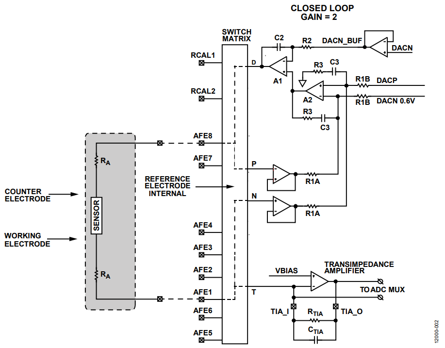
Figure 2. AFE Excitation Loop Block Diagram, 2-Wire Configuration.
Current Into T Node = (VAFE8 - VAFE1)/(RA + ZSENSOR + RA)
Voltage seen at ADC = Current into T Node × RTIA
where:
VAFE8 is the voltage at AFE8.
AAFE1 is the voltage at AFE1.
RA is the access resistance.
Amperometric Measurement Example
The example described in this section measures the current that flows from the counter electrode to the working electrode in a 2-wire sensor configuration with the RC sensor. This configuration is shown in Figure 3.
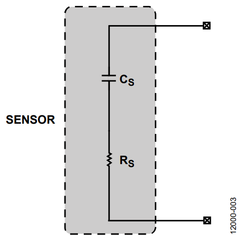
Figure 3. RC Sensor Model.
At time zero (t = 0), the counter electrode is held at midscale (1.1 V) and the working electrode is held at a common-mode voltage of 1.1 V (VBIAS) so that no current flows through the sensor. After 500 µs (t = 1), a 300 mV step voltage is applied to the counter electrode of the sensor (the DAC is configured to output 1.4 V).
The resultant current flows through the sensor and is converted to a voltage using the RTIA resistor and the TIA.
As shown in Figure 3, the CS series capacitor = 10 µF and the RS series resistor = 6.8 kΩ.
Theoretical Calculations
The RC time constant (τ) is the time constant of an RC circuit. This constant is the time required to charge or discharge the capacitor (C), through the resistor (R) by ~63.2% of the difference between the initial and final values. For an RC circuit,
τ = R × C
τ = 6.8kΩ × 10 µF = ~68ms
Because it is difficult to get high precision capacitors greater than 1 nF, a large capacitor is used.
This capacitor is a ±20%, X5R, dielectric device.
Figure 4 shows the ideal transfer function of the ADC for a TIA channel measurement with an RTIA of 7.5 kΩ.
0xD000 – 0x3000 = 0xA000 = 40960 decimal
200 µA/40960 = 4.88 nA
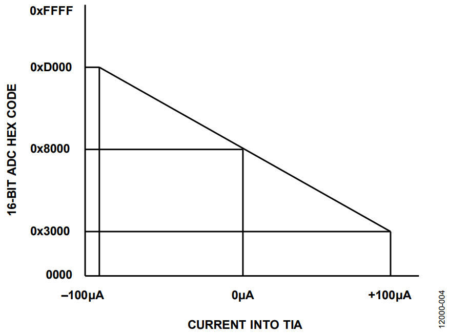
Figure 4. Ideal ADC Channel Transfer Function During Sensor/TIA Measurement for 7.5 kΩ RTIA.
This is equivalent to 1 LSB of the ADC when referred to the input current of the TIA, assuming an RTIA of 7.5 kΩ.
As calculated, 4340 codes is the number of codes to reach 63.2% of the maximum voltage, VMAX.
4.88 nA × 4340 = 21.1 µA
Amperometric Measurement Setup Using LabVIEW® GUI
The measurement is performed using the EVAL-ADuCM350 evaluation board for the ADuCM350 and the LabVIEW evaluation software (see Figure 5).
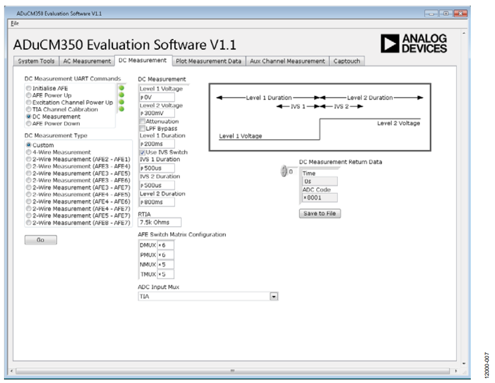
Figure 5. ADuCM350 LabVIEW GUI Using the EVAL-ADuCM350 Evaluation Kit.
In the example shown in this section, the device is setup in 2-wire mode with the D and P nodes connected to AFE6, and the T and N nodes connected to AFE5. This setup is completed in the AFE Switch Matrix Configuration pane, as shown in Figure 5.
The voltage step is programmed to increase from 0 V to 300 mV, sitting on the 1.1 V system common-mode voltage.
Enabling the current voltage switch (IVS) shunts the initial current spike seen by the TIA by shorting out RTIA and CTIA to prevent the receive stage from railing and losing stability.
The maximum voltage that the TIA channel can measure is 750 mV p-p. A 7.5 kΩ RTIA resistor is selected for a maximum current measurement of 100 µA.
Select DC Measurement in the DC Measurement UART Commands pane as shown in Figure 5. When the setup is complete, click Go to execute a measurement.
The following two options are available to view the data:
- Click the Plot Measurement Data tab and select the required plot from the dropdown list. Figure 6 shows the DC: ADC Code vs. Time plot.
- Click Save to File (see Figure 5) in the DC Measurement tab and open the file in Microsoft® Excel.
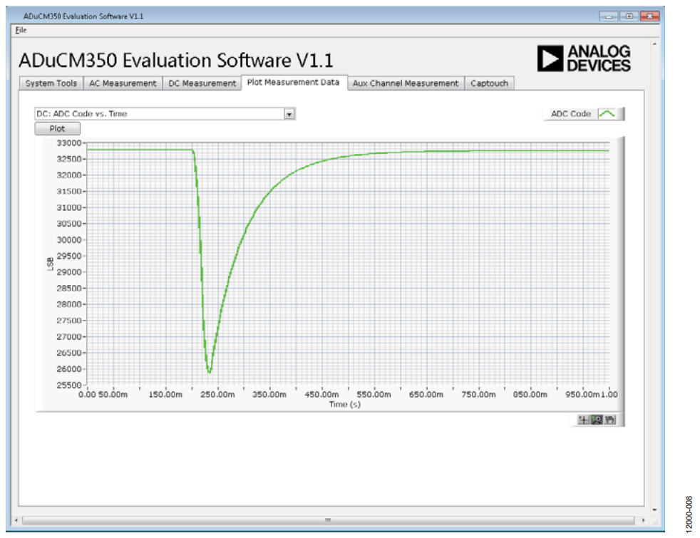
Figure 6. ADuCM350 LabVIEW GUI—Plotting ADC Results.
The RC step response can be observed after 0.2 seconds.
For large RC time factors, there is a settling time associated with closing the switches from all open to all closed as the RC goes from floating to being pulled to a known state.
This settling is not controllable in LabVIEW because there is a fixed wait time after closing the switches. This fixed wait time can be controlled in the IAR amperomtric example. See the Amperometic Measurement.c Example in SDK section for details.
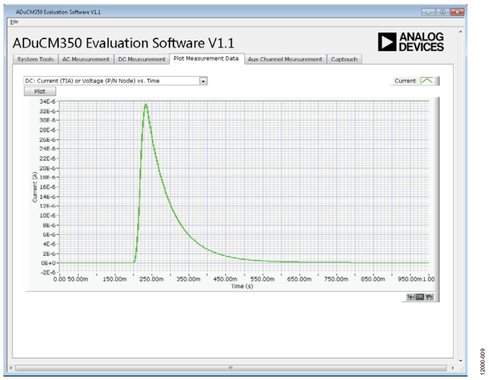
Figure 7. ADuCM350 LabVIEW GUI—Plotting Current Results.
Amperometric Measurement.c Example in SDK
Locate the amperometric example project in the ADuCM350BBCZ IAR-based software development environment. For example, C:\Analog Devices\ADuCM350BBCZ\EvalADUCM350EBZ\ examples\AmperometricMeasurement\iar\AmperometricMeasurement.eww.
See Figure 8 for details on setting up the measurement in IAR.
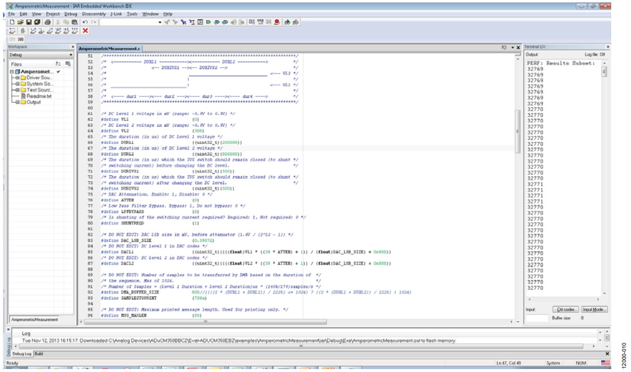
Figure 8. ADuCM350 Amperometric Setup in IAR.
User controllable variables consist of the following:
- DC Level 1
- DC Level 2
- Duration of dc Level 1
- Duration of dc Level 2
- IVS Switch 1 duration
- IVS Switch 2 duration
- Attenuation enable (DAC_ATTEN_EN)
- Power supply rejection filtering enable (LPFBYPASS)
- Enable IVS switching regulator
Apply a step voltage from DC Level 1 to DC Level 2. The IVS switch is enabled to prevent a current spike appearing on the TIA, which can potentially rail the signal (this is sensor dependent and a good practice to include).
The number of samples is limited by the AFE direct memory access (DMA) buffer size with a maximum limit of 1024. The ADC samples at 900 SPS and the buffer fills up after 1.38 sec.
This buffering limitation needs to be taken into account for the timing of the step and the resulting decay.
For large RC time factors, there is a settling time associated with closing the switches from all open to all closed as the RC goes from floating to being pulled to a known state. This settling time can be captured by ADC conversions unless a significant delay is allowed after closing the switches. In this example, a delay of 400 ms is chosen to allow the loop to settle completely (see Line 111 in Figure 9). If the switches are not changed when going from measurement mode to hibernate mode, this delay is not required after the initial command to close switches.
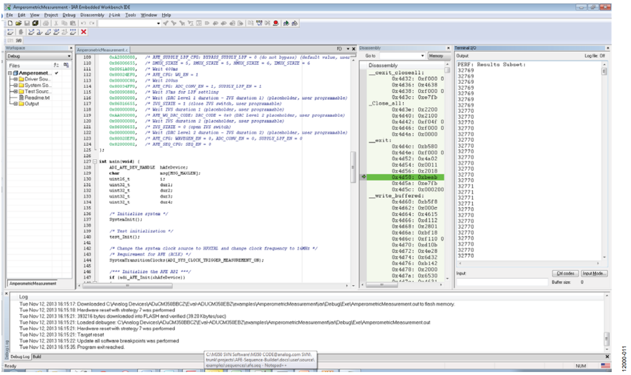
Figure 9. ADuCM350 Amperometric Example in IAR-Based Software Development Kit.
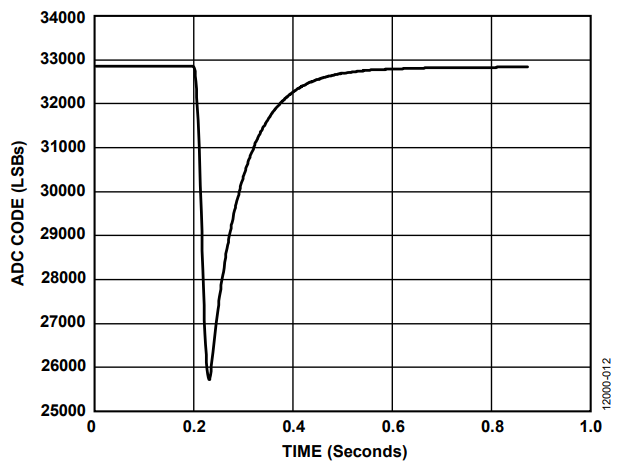
Figure 10. ADuCM350 IAR Results—ADC Code Copied from Terminal Input/Output Window.
Amperometric Measurements Results
RC Time Constant
Figure 6 shows the plot of the settling time (taken from actual measurements on the ADuCM350) in ADC LSBs from ~25900 codes to 32768 codes (midscale).
32768 – 25900 = 6868 codes
The time constant (τ) is the time elapsed after 63.2 % of VMAX has been reached.
63.2% × 6868 = 4340 codes
25900 + 4340 = 30240 codes
Figure 6 shows an actual measurement that takes ~65.6 ms to reach 63.2% of final settling voltage of midscale.
This measured value of ~65.6 ms is comparable to the theoretical value of 68 ms (see the Theoretical Calculations section for more details). The variance of the capacitor must be taken into account.
Current Seen By The ADC
Referring to the measured current plot in Figure 7, a maximum value of 33.5 µA is measured by the ADuCM350.
63.2% × 33.5 µA = 21.17 µA
This closely matches the theoretical measurement of 21.1 µA (see the Theoretical Calculations section for more details).
Notice that a small range of the full ADC range is used in this example. To increase the range of the ADC, the following options are available:
- Increase the step voltage magnitude. This can be limited for certain electrochemical cells.
- Increase the RTIA value, which reduces the measurable current range. The switch matrix can be configured so that the user can switch in various RTIA values if a programmable gain type architecture is required.
- Considering the very slow decay of this particular sensor, another option is to use some moving averaging of the 900 SPS ADC data to increase resolution from 16 bits to 17 bits/18 bits.