AN-1237: Precise Control of I/Q Modulator Output Power Using the ADL5386 Quadrature Modulator and the AD5621 12-Bit DAC
Circuit Function And Benefits
This circuit provides upconversion of I/Q modulated data and automatic power control of the RF/IF carrier level. The output power is set by a 12-bit digital-to-analog converter (DAC) and can be precisely set over a linear-in-dB range of up to 30 dB. Stability over temperature is typically ±0.2 dB from −40°C to +85°C. Figure 1 shows operation at an output frequency of 350 MHz; however, the circuit operates from 50 MHz to 2.2. GHz.
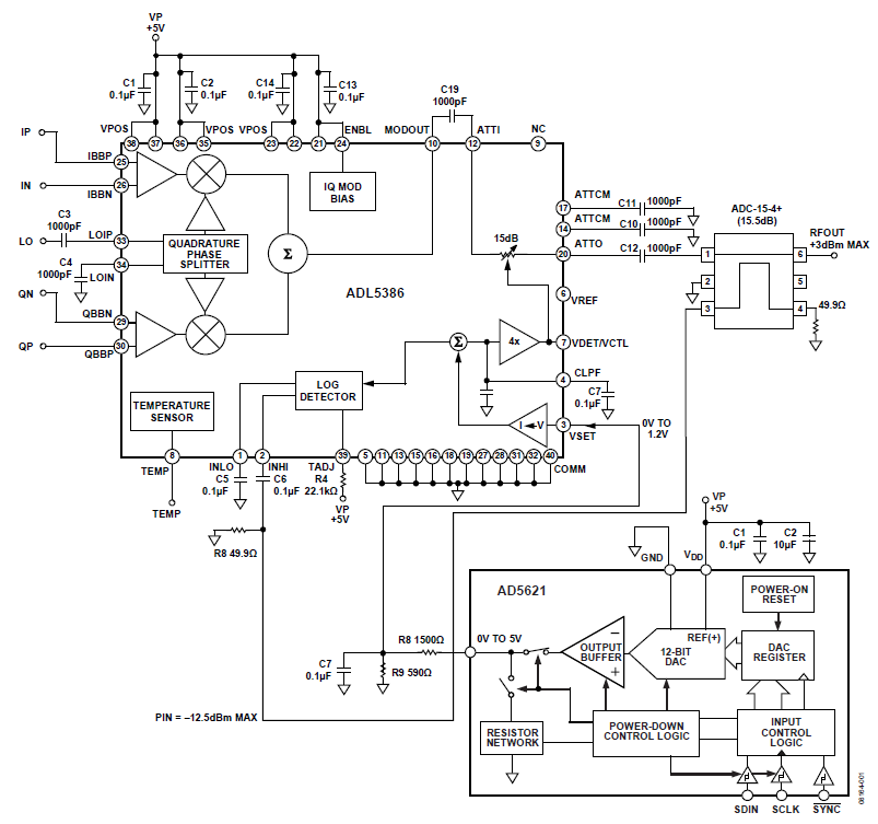
Figure 1. Diagram of System (Simplified Schematic).
Circuit Description
| Product | Description |
| ADL5386 | 50 MHz to 2200 MHz quadrature modulator with integrated detector and VVA |
| AD5621 | 2.7 V to 5.5 V, 12-bit nanoDAC® with SPI interface |
The ADL5386 quadrature modulator is comprised of three distinct functional blocks: an I/Q modulator, a voltage variable attenuator (VVA), and a logarithmic RF power detector/controller (log amp).
The output of the I/Q modulator (MODOUT) is ac-coupled to the input of the VVA (ATTI). A portion of the output signal from the VVA (ATTO) is coupled back to the input of the log amp. This can be done with a power splitter or with a directional coupler. In this example, a Mini-Circuits ADC-15-4+ directional coupler is used. The maximum RF input power to the detector must not exceed approximately −10 dBm because the log amp transfer function loses some linearity and temperature stability above this input RF power level. In the example shown, a maximum output power from the VVA/modulator of 3 dBm is desired. The coupling factor of the directional coupler is 15.5 dB at 350 MHz. This results in a maximum input level to the log amp of −12.5 dBm, well under the recommended maximum.
The input signal to the detector produces a current that is drawn from the summing node (Pin CLPF) into the detector block. A setpoint voltage from the DAC is applied to the VSET pin. Internally, this voltage is converted into a current that is pumped into the same summing node. If these two currents are not equal, the net current flows into or out of the CLPF capacitor on Pin 4. This changes the voltage on the CLPF node which, in turn, changes the voltage on the VDET/VCTL pin. This pin is internally connected to the attenuation control pin of the VVA. Therefore, the attenuation control voltage on Pin 7 (VDET/VCTL) increases or decreases until the ISET and IDET currents match. When this equilibrium is reached, the voltage on CLPF (and thereby on the control voltage node of the VVA) is held steady. At this point, the desired output power of the VVA/modulator matches the setpoint voltage from the DAC.
Figure 2 shows the resulting closed-loop transfer function; that is, output power at 350 MHz (on ATTO) vs. setpoint code from the AD5621 DAC. There is a well-controlled, linear-in-dB relationship between the RF output power and the voltage from the DAC over a range of approximately 30 dB. This contrasts with the open-loop transfer function of the VVA, which is not well-controlled or linear-in-dB (see the ADL5386 data sheet, Figure 23, Figure 24, Figure 26, and Figure 27).
To cover the output power range shown, a setpoint voltage range from 0.6 V to 1.3 V is required at the VSET input of the ADL5386 log detector/controller. With the AD5621 12-bit DAC powered from the same 5 V that powers the ADL5386 I/Q modulator, it can provide a much larger output swing from 0 V to 5 V. As a result, it makes sense to scale down the DAC output voltage so that the control resolution is optimized. To scale 5 V down to 1.3 V, a 1500 Ω/590 Ω resistor divider is chosen. This ensures that the DAC is not too heavily loaded (nominal specified load is 2 kΩ) but is also a small enough resistance that the input impedance of the VSET input on the ADL5386 (33 kΩ) does not affect the voltage division. A shunt capacitor has also been added to this network to filter out broadband noise and glitches from the DAC.
Figure 2 also shows a plot of the linearity of the transfer function in dB. The linearity is calculated by measuring the slope and intercept of the transfer function using the POUT data and the DAC codes. The calculations are performed using data in the output power range from approximately 0 dBm to −20 dBm.
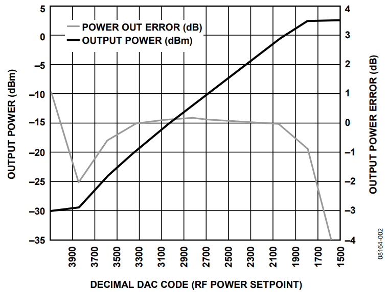
Figure 2. Output Power Transfer Function and Linearity Error.
This yields an idealized transfer function of
POUT_IDEAL = SLOPE × CODESET + INTERCEPT
The error in decibels is given by
ERROR (dB) = POUT − POUT_IDEAL
To obtain the precise output power control shown in Figure 2, the circuit must be calibrated when the equipment is in production. A typical procedure is as follows:
- Connect an RF power meter to the ATTO pin. RF power can also be measured at the outputs of subsequent stages.
- Apply the baseband modulated signal to the I and Q inputs. This signal is generally provided by a dual DAC. The level of this signal is not critical; however, it must be large enough so that the desired maximum output power can be reached when the VVA is at or close to minimum attenuation.
- Assuming that the coupling factor was chosen so that the maximum power at the input to the detector is approximately −12 dBm when the system is at maximum output power, apply a code to the DAC that gives a VSET voltage corresponding to this input level. To determine the relationship between VSET and the input power to the detector, see Figure 29 to Figure 32 in the ADL5386 data sheet.
- Measure and note the output power on the RF power meter (PHIGH). Note the DAC code that results in this power level (CODEHIGH).
- Now by increasing VSET, reduce the output power to approximately the bottom end of the desired output power range (−25 dBm, setpoint voltage is approximately 1.25 V).
- Again, measure the output power on the RF power meter (PLOW) and note the corresponding DAC code (CODELOW).
- Calculate the SLOPE and Y-axis INTERCEPT of the POUT
vs. VSET transfer function
SLOPE = (PHIGH − PLOW)/(CODEHIGH − CODELOW)
INTERCEPT = PHIGH − (SLOPE × CODEHIGH) - The calculated slope and intercept must be stored in the nonvolatile RAM in the equipment.
- When the equipment is in operation, the required code to
provide a desired output power (PX) can be calculated by
CODEX = (PX − INTERCEPT)/SLOPE
It is important to note that this algorithm does not rely on precise power or voltage levels being set during the calibration. As long as the calibration is performed using power and voltage levels that are within the linear operating range of the detector, all that matters is that the DAC codes are noted and that the output RF power is measured precisely using the RF power meter.
Alternatively, if the circuit must provide a single, steady output power to compensate for device-to-device variations in the baseband signal level and gain of the I/Q modulator, a simpler procedure can be employed as follows:
- Adjust the VSET voltage using the DAC until the exact desired output is measured on the RF power meter.
- Note and store the resulting DAC code (CODE1).
- When the equipment is in operation in the field, simply load the DAC with CODE1.
This circuit was implemented by connecting the following evaluation boards:
- ADL5386 evaluation board (ADL5386-EVALZ)
- Mini-Circuits Evaluation Board (TB-05) along with Mini-Circuits directional coupler (ADC-15-4)
- AD5621 evaluation board (EVAL-AD5621EBZ)
The EVAL-AD5621EBZ ships with software that allows it to be easily programmed through the USB port of a PC. Because the ADL5386-EVALZ and EVAL-AD5621EBZ use SMA and SMB connectors, respectively, the DAC to VSET interconnect was implemented with clip leads. Alternatively, an SMA to SMB adapter can be used.
The circuit must be constructed on a multilayer printed circuit board (PCB) with a large area ground plane. Proper layout, grounding, and decoupling techniques must be used to achieve optimum performance (see Tutorial MT-031, Grounding DataConverters and Solving the Mystery of AGND and DGND and Tutorial MT-101, Decoupling Techniques).
Common Variations
It is not required to place the directional coupler directly at the output of the VVA. For example, if the I/Q modulator is followed in the signal chain by a filter and/or amplifier, the coupler can be placed after these components. This results in the elimination of RF power uncertainty caused by the device-to-device variations and temperature drift of these devices. Because the detector on the ADL5386 I/Q modulator chip works well at frequencies up to and beyond 2.2 GHz, upconverting mixers can also be taken inside the loop. If the RF power level is being controlled is higher than the recommended maximum detector input level plus the coupling factor, place additional attenuation between the coupler and the detector.
In the previous example, a relatively large filter capacitor (CLPF) sets the response time of the circuit to changes in input power or to the setpoint voltage. To decrease the response time, the value of CLPF can be reduced. However, reducing the value of this capacitor causes signal distortion if the loop becomes fast enough to respond to the modulated envelope of the output signal. In addition, reducing the filter capacitor increases the broadband noise transfer from the detector to the VVA. This, in turn, results in a higher output noise floor.
A number of other DAC options exist. The AD5620 is a single, 12-bit DAC that contains an on-board voltage reference. If additional control voltages are required for other points in the circuit, the AD5623R dual, 12-bit DAC or the AD5624R quad DAC can be chosen. If an I2 C serial interface is required, the AD5622 (single, 12-bit), AD5627R (dual, 12-bit), or AD5625R (quad, 12-bit) can be used.
In addition, the AD7294 is worth considering. In addition to providing four 12-bit DAC outputs, this subsystem chip includes four uncommitted ADC channels, two high-side current sense inputs, and three temperature sensors. Current and temperature measurements are digitally converted and available to read over the I2 C interface. A device like this may be used to control the AGC input of the ADL5386 if a large number of other control and monitoring points were required in the system (for example, a combined radio and high powered amplifier unit).
LEARN MORE
MT-077 Tutorial, Log Amp Basics. Analog Devices.
MT-078 Tutorial, High Frequency Log Amps. Analog Devices.
MT-079 Tutorial, Analog Multipliers. Analog Devices.