AN-1137: ADE7816 Theory of Operation
Introduction
The ADE7816 is a multichannel energy metering IC that can measure up to six current channels and one voltage channel simultaneously. The ADE7816 provides active and reactive energy, along with current and voltage rms readings on all channels. A variety of power quality features, including no load, reverse power, and angle measurements, are also provided. The ADE7816 is suitable for use in a variety of metering applications, including smart electricity meters, power distribution units, and in-home energy monitors.
This application note provides theoretical information about the ADE7816 energy and rms calculations and should be used as a supplementary document to the ADE7816 data sheet.
Figure 1 shows the signal path for one voltage and current channel pair on the ADE7816. The ADE7816 has six separate energy signal paths and, therefore, this signal path is duplicated six times. Details are provided on each block of the data path in sequential order, focusing on the theory behind the measurement. The application note is divided into two sections: the first section provides details about the analog conversion and filter, and the second describes the digital signal processing.
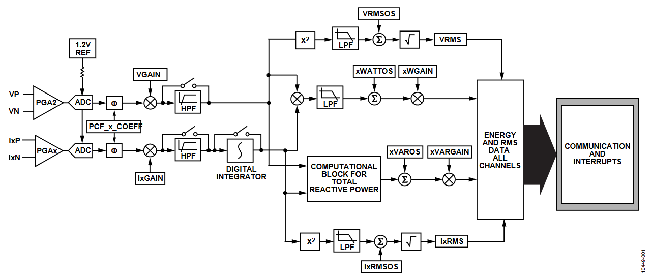
Figure 1. Signal Path.
Analog Conversion and Filtering
This section focuses on the analog portion of the ADE7816 energy meter and the associated filtering, which includes the analog-to-digital conversion, high-pass filter, and integrator (current channel only). Figure 2 and Figure 3 show the signal path of the analog converter and filter portion of the current and voltage channels, respectively. As shown, the current and voltage channel signal paths are identical, with the exception of the digital integrator that is included only on the current channels. The integrator allows direct connection to Rogowski coil current sensors (see the Digital Integrator (Current Channels Only) section for more details).
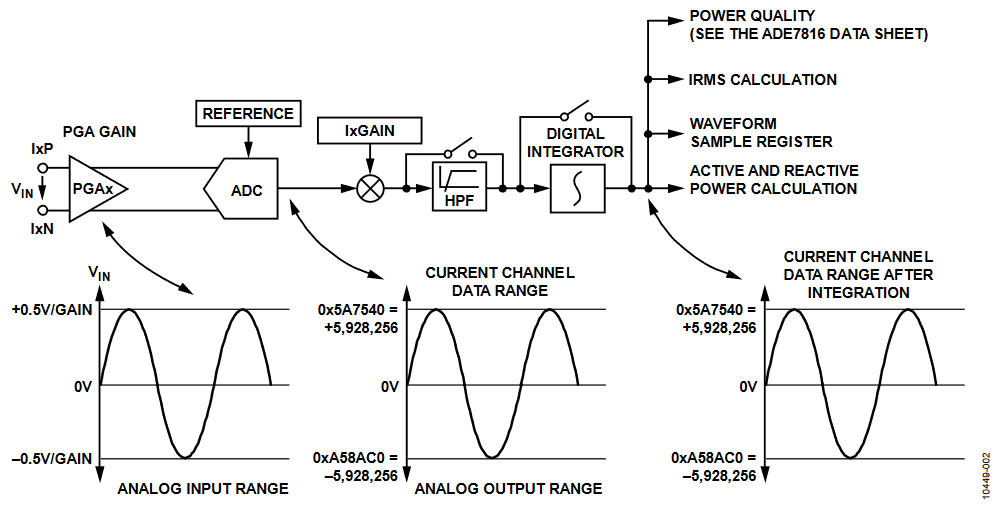
Figure 2. Current Channel Signal Path.
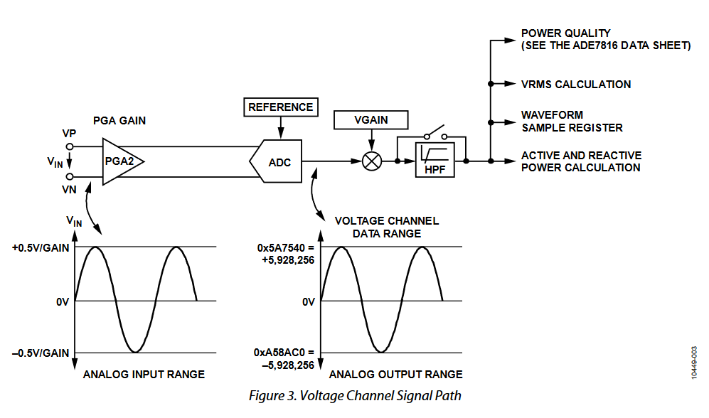
Figure 3. Voltage Channel Signal Path.
Analog-to-Digital Conversion
The ADE7816 includes sigma-delta (Σ-Δ) analog-to-digital converters (ADCs) to convert the incoming analog signal into a digital bit stream. When the ADE7816 is fully powered, all ADCs are active.
For simplicity, the block diagram in Figure 4 shows a first-order Σ-Δ ADC. The converter is composed of the Σ-Δ modulator and the digital low-pass filter.
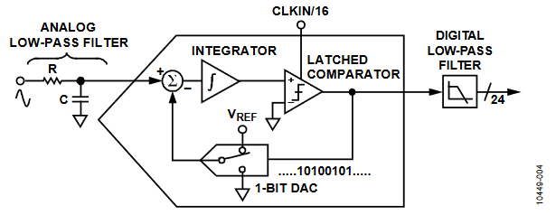
Figure 4. First-Order Σ-∆ ADC.
A Σ-Δ modulator converts the input signal into a continuous serial stream of 1s and 0s at a rate that is determined by the sampling clock. In the ADE7816, the sampling clock is equal to 1.024 MHz (CLKIN/16). The 1-bit DAC in the feedback loop is driven by the serial data stream. The DAC output is subtracted from the input signal. If the loop gain is high enough, the average value of the DAC output (and, therefore, the bit stream) can approach that of the input signal level. For any given input value in a single sampling interval, the data from the 1-bit ADC is virtually meaningless. A meaningful result can be obtained only when a large number of samples is averaged. This averaging is carried out in the second part of the ADC, the digital low-pass filter. By averaging a large number of bits from the modulator, the low-pass filter can produce 24-bit data-words that are proportional to the input signal level.
The Σ-Δ converter uses two techniques to achieve high resolution from what is essentially a 1-bit conversion technique. The first is oversampling. Oversampling means that the signal is sampled at a rate (frequency) that is many times higher than the bandwidth of interest. For example, the sampling rate in the ADE7816 is 1.024 MHz, and the bandwidth of interest is 40 Hz to 2 kHz. Oversampling has the effect of spreading the quantization noise (noise due to sampling) over a wider bandwidth. With the noise spread more thinly over a wider bandwidth, the quantization noise in the band of interest is lowered, as shown in Figure 5. However, oversampling alone is not enough to improve the signal-to-noise ratio (SNR) in the band of interest. For example, an oversampling factor of 4 is required just to increase the SNR by a mere 6 dB (one bit). To keep the oversampling ratio at a reasonable level, it is possible to shape the quantization noise so that the majority of the noise lies at the higher frequencies. In the Σ-Δ modulator, the noise is shaped by the integrator, which has a high-pass type of response for the quantization noise. This is the second technique used to achieve high resolution. The result is that most of the noise is at the higher frequencies, where it can be removed by the digital low-pass filter. This noise shaping is shown in Figure 5.
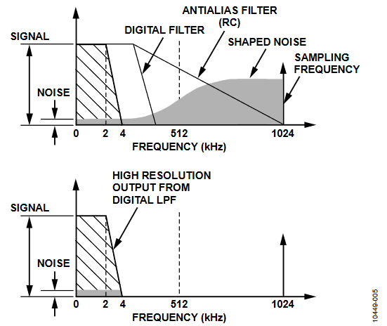
Figure 5. Noise Reduction Due to Oversampling and Noise Shaping in the Analog Modulator.
ADC Transfer Function
All ADCs in the ADE7816 are designed to produce a similar 24-bit, signed output code for the same input signal level. The 24-bit, signed output code is available at a fixed rate of 8 kSPS (thousand samples per second). With a full-scale input signal of 0.5 V and an internal reference of 1.2 V, the ADC output code is approximately 5,928,256 (0x5A7540), as shown in Figure 2 and Figure 3. The code from the ADC can vary between 0x800000 (−8,388,608) and 0x7FFFFF (+8,388,607); this is equivalent to an input signal level of ±0.707 V. However, for specified performance, do not exceed the nominal range of ±0.5 V; ADC performance is guaranteed only for input signals that are lower than ±0.5 V.
High-Pass Filters (HPFs)
The ADC outputs can contain a dc offset. This offset can create errors in power and rms calculations. High-pass filters (HPFs) are placed in the signal path of the phase and neutral currents and of the phase voltages. The HPFs eliminate any dc offset on the current or voltage channel and have a cut-off frequency of 0.2 Hz.
Digital Integrator (Current Channels Only)
The internal digital integrator is designed for use with a Rogowski coil or other di/dt sensor. A di/dt sensor detects changes in the magnetic field caused by the ac current. Figure 6 shows the principle of a di/dt current sensor.
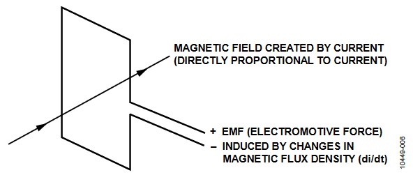
Figure 6. Principle of a di/dt Current Sensor.
The flux density of a magnetic field that is induced by a current is directly proportional to the magnitude of the current. The changes in the magnetic flux density passing through a conductor loop generate an electromotive force (EMF) between the two ends of the loop. The EMF is a voltage signal that is proportional to the di/dt of the current. The voltage output from the di/dt current sensor is determined by the mutual inductance between the current-carrying conductor and the di/dt sensor.
Due to the di/dt sensor, the current signal must be filtered before it can be used for power measurement. On each current channel, there is a built-in digital integrator to recover the current signal from the di/dt sensor. The digital integrator is disabled by default, but it can be enabled by setting Bit 0 (INTEN) of the CONFIG register (see the ADE7816 data sheet). Figure 7 and Figure 8 show the magnitude and phase response of the digital integrator.
When the digital integrator is switched off, the ADE7816 can be used directly with a conventional current sensor, such as a current transformer (CT).
Note that the integrator has a −20 dB/dec attenuation and approximately −90° of phase shift. When combined with a di/dt sensor, the resulting magnitude and phase response should be a flat gain over the frequency band of interest. However, the di/dt sensor has a 20 dB/dec gain associated with it and generates significant high frequency noise. An antialiasing filter of at least the second order is needed to avoid noise aliasing back in the band of interest when the ADC is sampling (see the ADE7816 data sheet).
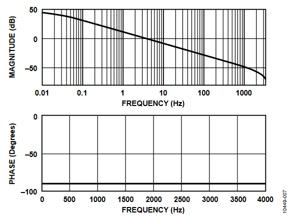
Figure 7. Combined Gain and Phase Response of the Digital Integrator.
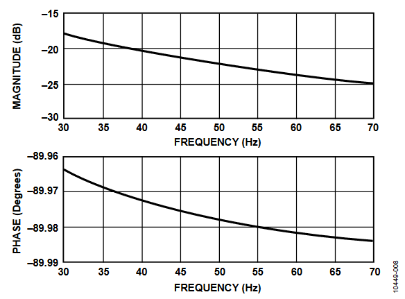
Figure 8. Combined Gain and Phase Response of the Digital Integrator (30 Hz to 70 Hz).
Digital Processing
The ADE7816 contains a fixed function digital signal processor (DSP) that computes all power and rms values. It contains program memory ROM and data memory RAM.
The program that is used for the power and rms computations is stored in the program memory ROM, and the processor executes it every 8 kHz.
Total Active Power Calculation
Electrical power is defined as the rate of energy flow from source to load, and it is given by the product of the voltage and current waveforms. The resulting waveform is called the instantaneous power signal, and it is equal to the rate of energy flow at every instant of time. The unit of power is the watt or joules/sec. If an ac system is supplied by a voltage, v(t), and consumes the current, i(t), and each of them contains harmonics, then:

where:
Vk, Ik are rms voltage and current, respectively, of each harmonic.
φk, γk are the phase delays of each harmonic.
The instantaneous power in an ac system is as follows:
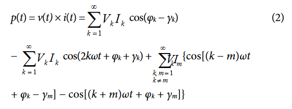
The average power over an integral number of line cycles (n) is given by the expression that is shown in Equation 3.

where:
T is the line cycle period.
P is referred to as the total active or total real power.
Note that the total active power is equal to the dc component of the instantaneous power signal p(t) in Equation 2; that is,

This is the expression used to calculate the total active power in the ADE7816 for each channel.
The ADE7816 computes the total active power on each channel by first multiplying the current and voltage signals on each. Next, the dc component of the instantaneous power signal is extracted using a low-pass filter (LPF), as shown in Figure 11.
If the voltage and currents contain only the fundamental component, are in phase (that is, φ1 = γ1 = 0), and correspond to full-scale ADC inputs, then multiplying them results in an instantaneous power signal that has a dc component, V1 × I1, and a sinusoidal component, V1 × I1 cos(2ωt). Figure 9 shows the corresponding waveforms.
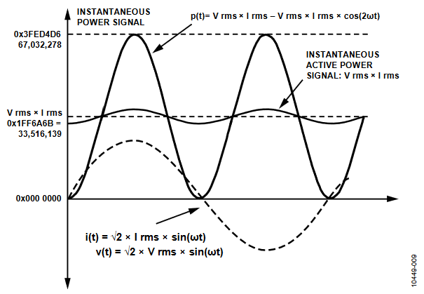
Figure 9. Active Power Calculation.
Because the LPF does not have an ideal brick wall frequency response (see Figure 10), the active power signal has some ripple due to the instantaneous power signal. This ripple is sinusoidal and has a frequency that is equal to twice the line frequency. Because the ripple is sinusoidal in nature, it is removed when the active power signal is integrated over time to calculate the energy.
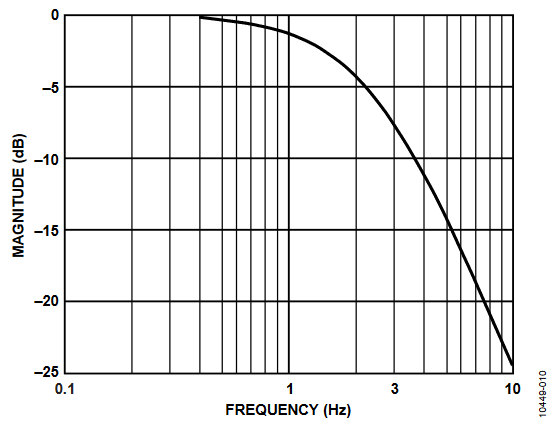
Figure 10. Frequency Response of the LPF Used to Filter Instantaneous Power in Each Phase.

Figure 11. Active Energy Data Path.
Active Energy Calculation
As previously stated, power is defined as the rate of energy flow. This relationship can be expressed mathematically as:

Conversely, energy is given as the integral of power, as follows:

Active energy accumulation is a signed operation. Negative energy is subtracted, and positive energy is added to total energy accumulation.
The ADE7816 calculates the energy by accumulating the power over time. This discrete time accumulation or summation is equivalent to integration in continuous time, following the description in Equation 6.

where:
n is the discrete time sample number.
T is the sample period.
The accumulation is performed in two stages (see Figure 11): first, by an internal threshold and, next, in an external register. See the ADE7816 data sheet for more information on setting the internal threshold.
Reactive Power
The ADE7816 can compute the total reactive power on each channel. Reactive power integrates the fundamental and harmonic components of the voltages and currents. A load that contains a reactive element (inductor or capacitor) produces a phase difference between the applied ac voltage and the resulting current. The power associated with the reactive elements is called reactive power, and its unit is the var. Reactive power is defined as the product of the voltage and current waveforms when all harmonic components of one of these signals are phase shifted by 90°.
Equation 7 gives an expression for the instantaneous reactive power signal in an ac system when the phase of the current channel is shifted by +90°.


where i'(t) is the current waveform with all harmonic components phase shifted by 90°.
Next, the instantaneous reactive power, q(t), can be expressed as:
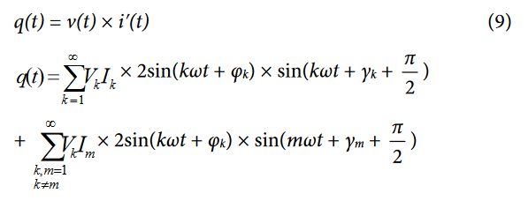
Note that q(t) can be rewritten as:
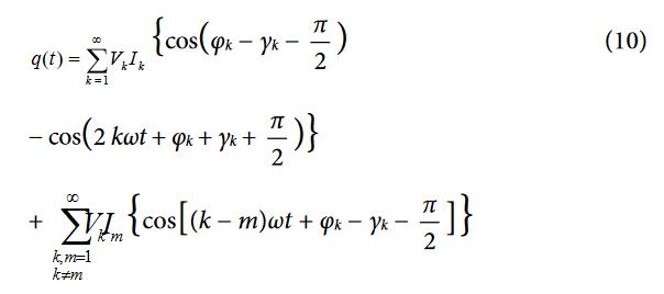
The average total reactive power over an integral number of line cycles (n) is given by the expression in Equation 11.

where:
T is the period of the line cycle, and Q is referred to as the total reactive power. Note that the total reactive power is equal to the dc component of the instantaneous reactive power signal, q(t), in Equation 10; that is,

This relationship is used to calculate the total reactive power for each channel. The instantaneous reactive power signal, q(t), is generated by multiplying each harmonic of the voltage signals by the 90° phase-shifted corresponding harmonic of the current in each phase.

Figure 12. Reactive Energy Data Path.

Figure 13. IRMS Signal Path.
Reactive Energy Calculation
Reactive energy is defined as the integral of reactive power.
Reactive Energy = ∫q(t)dt (12)
Reactive energy accumulation is a signed operation. Negative energy is subtracted from the reactive energy contents.
Similar to active power, the ADE7816 achieves the integration of the reactive power signal in two stages (see the ADE7816 data sheet).
RMS
Root mean square (rms) is a measurement of the magnitude of an ac signal. Its definition can be both practical and mathematical. Defined practically, the rms value assigned to an ac signal is the amount of dc that is required to produce an equivalent amount of power in the load. Mathematically, the rms value of a continuous signal, f(t), is defined as follows:

For time sampling signals, rms calculation involves squaring the signal, taking the average, and obtaining the square root.

Equation 14 implies that for signals containing harmonics, the rms calculation contains the contribution of all harmonics, not only the fundamental. The ADE7816 uses a low-pass filter to average the square of the input signal and then takes the square root of the result. This concept is explained mathematically in the following formulas:

Then:

After the LPF and the execution of the square root, the rms value of f(t) is obtained by:

The rms calculation on the current and voltage channel is performed using the same method. See Figure 13 for a block diagram of the Irms measurement.
