This applications note introduces a novel and tested topology
for boost converters with moderately high boost ratios (such as
10:1 to 50:1). This topology overcomes many of the disadvantages
presented by other methods. The benefits of this design approach
include the following:
Significant reduction in voltage stress on the main and
rectifier switches without any accompanying significant
increase in current stress. This widens and improves the
choices in MOSFETs and Schottky rectifiers, for which
high voltage is often a disadvantage.
Moderate (as opposed to very high) pulse-width modulation
(PWM) duty cycles that allow continuous conduction
mode (CCM) operation and make feedback loop compensation easier.
Better efficiency due to: moderate duty cycles, lower
voltage MOSFETs and rectifiers, and reduced switching
losses due to reduced peak-to-peak voltage swing.
Reduced noise due to reduced energy in switch node
capacitance. In addition, high frequency emissions may be
reduced because multiple inductor energy discharge paths
seem to dampen high frequency ringing.
Scope
The purpose of this application note is to introduce circuit
designers to a novel and useful power conversion topology. It
deals with voltages ranging from as low as approximately 1.8 V
on the input, up to voltages as high as perhaps 500 V on the output.
This application note compares the subject method with other
methods for obtaining high boost ratios, and it presents a tested
design example. It also covers information on design variations
and component considerations. It is not intended to be a complete
or exhaustive design manual. Design engineers requiring assistance
with any aspect of designing with this topology are encouraged
to contact Applications Engineering at www.analog.com.
Introduction—A Look at Alternative Topologies
There are several dc-to-dc converter topologies for obtaining
relatively high (over 10:1) boost ratios. These topologies include:
Simple boost
Charge pump multiplied boost
Tapped inductor boost
Simple Boost
Figure 1. Simple Boost
The simple boost operating parameters are listed in Table 1.
The advantages of a simple boost topology include:
It is the simplest schematic design with the fewest parts.
It is highly efficient when used with low-to-moderate boost ratios.
The disadvantages of a simple boost topology include:
High boost ratios impose both high voltage and high current stress on Q1. The MOSFET must be rated for full output voltage and relatively high current (translating to low RDS on). This results in a large MOSFET die which tends to be expensive and requires a strong gate driver. Switching losses are likely to be high due to large voltage transitions on the large die transistor.
High voltage on the rectifier may preclude the use of common Schottky diodes; therefore, a lossier ultrafast type may be needed. Large boost ratios require high duty cycle.
High duty cycles and ultrafast diodes can both point to discontinuous conduction mode (DCM) which usually increases conduction loss.
Table 1. Operating Parameters for Simple Boost Converter
Parameter
Equation
Numerical Value for 12 V into 150 V Output at 200 mA
Comment
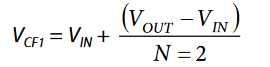
Voltage CF1
Not applicable
Not applicable
No such node in this topology
CCM Duty Cycle D
D = (VOUT − VIN)/VOUT
92%
Q1 Peak Volts
Q1 VPEAK = VOUT
150 V
Q1 Amps RMS (Large L)
2.6 A
Approximation is very close for low inductor ripple
D1 Peak Volts
D1 VPEAK = VOUT
150 V
Charge Pump Multiplied Boost
The charge pump multiplied boost operating parameters are listed
in Table 2. This example uses N = 2 stages.
Figure 2. Charge Pump Multiplied Boost with Two Stages
The advantages of the charge pump multiplied boost topology
are as follows:
They are an economical choice for high output voltage and low output current.
They provide high boost ratios with improved duty cycle and reduced voltage stress on the rectifiers and main switch.
The disadvantages of the charge pump multiplied boost topology are as follows:
Each charge pump multiplier stage requires two added series diodes, which contribute to loss from forward voltage drop.
Unlike the other topologies shown, a charge pump is not a true switcher in that it does not use inductor(s) as a current source(s) to limit the peak current in the pump capacitor(s). The pump capacitors need to be large in value to avoid causing high peak currents and significant cyclic droop.
High peak currents tend to increase rms switch current and can corrupt current mode control waveforms.
For these reasons, charge pump multipliers are best confined to applications where output current does not exceed 50 mA to 100 mA.
Table 2. Operating Parameters for Charge Pump Multiplied Boost Converter
Parameter
Equation
Numerical Value for 12 V into 150 V Output at 200 mA
Comment
Voltage at CF1
VCF1 = VOUT/(N = 2)
75 V
CCM Duty Cycle D
D = (VCF1 – VIN)/VCF1
84%
Q1 Peak Volts
Q1 VPEAK = VCF1
75 V
Q1 Amps RMS (Assuming Large L1 and CP1)
2.51 A
D(n) Peak Volts
D(n) VPEAK = VCF1
75 V
Same for all diodes
Table 3. Operating Parameters for Tapped Inductor Boost Converter
Parameter
Equation
Numerical Value for 12 V into 150 V Output at 200 mA, N1 = N2
Comment
Voltage CF1
Not applicable
Not applicable
No such node in this topology
CCM Duty Cycle D
85.19%
Q1 Peak Volts
81 V
Does not include leakage L spikes
Q1 Amps RMS (Large L)
2.492 A
Approximation is very close for low inductor ripple
D1 Peak Volts
D1 VPEAK = VOUT + (N2 × VIN/N1)
162 V
Does not include leakage L spikes
Tapped Inductor Boost
The tapped inductor boost operating parameters are listed in
Table 3. In this example, N1 = N2. The tapped inductor can
also be described as an autotransformer with a gapped core.
Figure 3. Tapped Inductor Boost
The advantage of a tapped inductor boost topology is that a
good design can provide high output voltage with improved
duty cycle and reduced voltage stress on the main switch.
The disadvantages of the tapped inductor boost topology are:
This technique cannot reduce voltage stress on the output rectifier. In fact, for the same output voltage, the voltage stress on the output rectifier is worse than that obtained with a simple boost.
Tapped inductor boost converters suffer from effects of transformer leakage inductance. The leakage inductance causes voltage spikes and ringing which causes EMI and increases voltage stress on both the MOSFET and the output rectifier. These effects can be controlled with snubbers; however, such remedies waste power.
The high voltage stress on the output rectifier frequently precludes the use of Schottky diodes; therefore, ultrafast diodes with discontinuous conduction mode and lower efficiency are often indicated. In addition, the tapped inductor often needs to be custom manufactured.
Need for a Better Technique
All of the above techniques have significant drawbacks for
delivering significant power at large boost ratios. There is a
need for a converter topology that:
Can deliver high boost ratios with minimum voltage and current stress being imposed on the switches so that moderately-rated (for example, 30 V to 100 V range) MOSFETs and Schottky rectifiers may be used.
Can operate at moderate duty cycles (for example, less than 85% to 90%) for easier CCM and PWM control.
Are “true switchers” without the drawbacks (including low output current) of charge pumps.
Avoid the voltage spikes and ringing associated with transformer leakage inductance.
The single-ended primary inductance converter (SEPIC) multiplied boost converter achieves all of the above goals. The advantages are as follows:
Voltage stress on the main switch and rectifiers is reduced. This results in an improved set of component selection trade-offs for price and performance. Peak-to-peak voltage swing on the switch node is greatly reduced so that switching losses are reduced.
The duty cycle is much closer to symmetry, often enabling CCM with straightforward current mode control.
EMI and noise are reduced due to lower peak-to-peak voltage swing on the switch node, and also often due to reduced ringing caused by multiple inductor current discharge paths.
No ringing or voltage stress resulting from transformer leakage inductance.
None of the increased current stress or distorted current waveforms that charge pumps typically cause.
Table 4. Operating Parameters for SEPIC Multiplied Boost Converter
Parameter
Equation
Numerical Value for Example Above
Comment
Voltage CF1
81 V
CCM Duty Cycle D
85.19%
This figure is readily achieved by most controller ICs
Q1 Peak Volts
Q1 VPEAK = VCF1
81 V
Q1 VPEAK varies with VIN and VOUT and is higher than with charge pump multiplied boost.
Q1 Amps RMS (Large L)
2.492 A
The approximation is very close for low inductor ripple.
D(n) Peak Volts
D(n) VPEAK = VCF1
81 V
D(n) VPEAK varies with VIN and VOUT and is higher than with charge pump multiplied boost.
Total effective parallel inductance Lp (eff) using n discrete inductors
29 µH
The total effective parallel inductance determines ripple current through Q1 during D. It is possible for some of the inductor currents to pass through zero while the totaled waveform at Q1 is CCM.
Total effective parallel Lp (eff) inductance using one multiwinding coupled inductor
Use rated inductance for any one winding or for all windings connected in parallel
33 µH would be a good choice but is not shown in the example above.
Although coupled inductors tend to understress the output winding current, using one multiwinding component may save bill of material (BOM)/assembly cost or printed circuit board (PCB) space compared to several discrete inductors.
Peak-to-peak ripple current in Q1 during on time
710 mA
Note that the ripple current passing through Q1 is not represented by that in any one inductor winding.
Q1 Peak Amps (for CCM)
3.06 amps
Comparison Example of the SEPIC Multiplied Boost Converter
SEPIC Multiplied Boost
This example uses N = 2 stages. Inductor windings may be
discrete or coupled (in which case, inductance of windings
shown as L1 and L2 is identical).
The advantages of the SEPIC multiplied boost converter are:
Compared to a straight boost converting the same voltages, this technique provides a more symmetrical duty cycle and reduced voltage stress on the MOSFET and the rectifiers. Although having two diodes increases the total diode forward drop, lower peak reverse voltage per diode allows use of Schottky or types with lower VF (forward voltage) types, and the smaller peak-to-peak ac waveform reduces switching loss.
The SEPIC multiplied boost avoids the spikes and ringing that are caused by leakage inductance in a transformer. It is a “true switcher” that uses inductor windings as current sources and capacitors as voltage sources. It avoids the differentiated current spikes that are characteristic of charge pumps.
The disadvantages of the SEPIC multiplied boost technique are:
Increased number of series-connected rectifiers increases the total rectifier forward voltage drop. (This loss is usually outweighed by other efficiency advantages.)
Increased complexity and parts count.
None of the voltage multiplication techniques (including the
SEPIC multiplied boost) is particularly helpful when VIN and
VOUT are both high. For example, if the input is 140 V and the
output is 150 V, no number of multiplier stages N will reduce
the peak imposed on the diodes and MOSFET to less than 140 V.
The large number of stages will simply add more series windings
and diodes, thus increasing the cost and the total circuit losses.
Regardless of VOUT within the scope of this application note, if
the boost ratio is low, a simple boost is probably the best approach.
Derivation of the SEPIC Multiplied Boost Converter from Other Topologies
This section shows how the SEPIC multiplied boost converter is derived from the SEPIC and boost topologies.
Simple Boost Converter
This is one of the most basic converter topologies. It produces
VOUT > VIN.
Figure 5. Simple Boost Converter
Single-Ended Primary Inductance Converter (SEPIC)
The SEPIC is a member of the buck-boost family. VOUT and VIN
have the same polarity. Its primary application is where VIN can
vary above or below VOUT. Note that one end of L2 is grounded.
Both ends of L2 have an average dc voltage of 0 V.
Figure 6. SEPIC Converter
SEPIC with Added Boost Output
By adding a diode and output filter to the SEPIC, an additional
boost output can be obtained. Only one of the two outputs (either
the boost or the SEPIC) can be regulated while the other varies
with VIN; therefore, the usefulness of this dual output technique
is limited to special circumstances. However, both outputs are
delivered cleanly without corruption of key voltage or current
waveforms.
Figure 7. SEPIC Converter with Added Boost
SEPIC Multiplied Boost (N = 2)
This topology is based on the SEPIC with the added boost
output example. The only changes are that L2 is now connected
to the junction of D1 and CF1 (which was VOUT boost) instead
of to ground. The VOUT boost connection has been removed. L2
and the SEPIC stage are connected in dc series with the boost
output at CF1. Both ends of L2 have an average dc voltage equal
to the boost voltage on CF1.
Figure 8. SEPIC Multiplied Boost Converter with N = 2
Circuit Analysis of a Multistage SEPIC Multiplied Boost
Figure 9. SEPIC-Coupled Quadrupler Using Discrete Inductors and Series Capacitors
Some simplifying assumptions follow:
All components are perfect. The MOSFET and diodes have negligible forward drop and negligible off-state leakage current.
The inductor values are large so that inductor ripple current is negligible. The current through the inductors is relatively pure dc.
The capacitors function as dc voltage sources with negligible ripple. Therefore, the ac voltages on both ends of any given capacitor can be assumed to be identical.
Operation is continuous conduction mode with instantaneous transitions and no dead time.
There are no losses.
The following example was constructed to provide easy calculations. Requirements are that VIN = 10 V and VOUT = 170 V at 200 mA. In addition, the controlling IC switches the
MOSFET at 500 kHz.
The circuit operation was analyzed as follows:
By examination, it can be seen that the only dc current path from L1 to Q1 (the switch node) to the output is through L2 to L4 and D1 to D4. Therefore, L2 to L4 and D1 to D4 must all carry 200 mA dc. Note that L1 must be considered separately because it also passes current into Q1 (see Step 11 for L1 discussion).
Because the ac voltage waveform (not the dc component) on both ends of any capacitor is assumed identical, it can be seen that the ac waveform present at the switch node (that is the drain of Q1, the main switch) is replicated on both ends of CC2, CC3, and CC4. By visual analysis and inductor volt second balancing, it can be seen that if the switch node peaks at some boost value = VB volts above VIN, the voltage at the anode of D2 must likewise peak at VB volts above the voltage at the cathode of D1. Likewise, the voltage at the anode of D3 must peak at VB volts above that on the cathode of D2, and the voltage at the anode of D4 must peak at VB volts above that on the cathode of D3. All four stages have similar ac voltage waveforms; therefore, the VB voltage gain per stage is identical for each stage. The total voltage gain achieved (170 V – 10 V = 160 V) is divided evenly among the four stages.
The VB numerical expression is VCF1 = VIN + ((VOUT – VIN)/(N = 4)), which results in 50 V out of the first stage. Because each stage produces the same boost differential, each stage then produces 50 V − 10 V = 40 V of VB boost differential or gain. The four stages produce dc levels of 50 V dc, 90 V dc, 130 V dc, and 170 V dc, respectively.
Calculate the duty cycle based on inductor volt second balancing. D = (VCF1 − VIN)/VCF1 results in 80% duty cycle. (By comparison, a simple boost requires > 94% duty cycle to produce the same 10 V to 170 V voltage conversion.)
With the previous information, the ac voltage waveforms shown in Figure 9 in red can be constructed. The waveform at the anode of D1 has an 80% duty cycle, a peak-to-peak value of 50 V, and a dc average of 10 V = VIN). Diodes D2 to D4 each have the same ac waveform; however, the dc voltages are shifted by 40 V for each stage.
If D = 80%, D1 to D4 are only conducting during (1 − D) = 20% of the time. The average of 200 mA dc passing through D4 is actually embodied in a 20% duty cycle current pulse. If the current pulse waveforms have a dc average of 200 mA and a 20% duty cycle, the pulses must have an amplitude of 200 mA/20% = 1 A. It then follows that the current waveform in D1 to D4 is similar to that shown in Figure 10.
Figure 10. Current Waveform in Diode D1 through Diode D4
This waveform has a 1 A peak-to-peak ac component combined with a 200 mA dc offset. This combination is
consistent with the instantaneous current never getting below 0 A. The ideal diodes do not conduct reverse current. In fact, most modern Schottky diodes rated above 25 V come pretty close to this, with 100°C reverse current below 100 µA.
For D1, this diode current waveform is supplied by L1 and Q1. Q1 cannot source positive current, and the current through L1 is positive dc coming from the 10 V input. It follows that the 1 A level is supplied by the inductor to D1 when Q1 is off during (D − 1) and diverted to ground through Q1 when it is on during D. The total amount of current passing through L1 and Q1 is calculated in Step 11.
Because capacitors cannot pass dc current, it is known that CC4 can only provide ac. At the same time, L4 supplies 200 mA of relatively pure dc. It is helpful to compare the current sources feeding D4 with those feeding D1. For both D4 and D1, the dc current component is supplied by the respective inductor windings. For D1, the ac current component is supplied by Q1, while for D4, the ac component is supplied by CC4.
The current waveform through CC4 is similar to that shown in Figure 11.
Figure 11. Current Waveform Through CC4
This ac only current in CC4 does not pass through L3, but instead gets to CC4 via CC2 and CC3. This ac current adds to the dc component from L4 to produce the common diode current waveform shown in Figure 10. This diode current is averaged by the output filter capacitor that is comprised of CF1 to CF4 connected in series.
It is a similar situation for D3, CC3, and L3, with one important difference. While L2, L3, and L4 all pass the same 200 mA dc in series, D3 and D4 each require their own 1 A p-p ac pulse. These ac current pulses are additive:
CC4 passes 1 A p-p for D4
CC3 passes 1 A p-p for D3 + 1 A p-p for D4 = 2 A p-p
CC2 passes 1 A p-p for D2 + 1 A p-p for D3 + 1 A p-p for D4 = 3 A p-p
The current feeding CC2 all originates from the combination of Q1 and L1. The current waveforms through CC2 and CC3 are similar to those shown in Figure 13.
In addition to the ac current for CC2, Q1 and L1 also supply all of the ac + dc passing through D1 (See the current waveform common to all four diodes shown in Figure 10). The total waveform supplied by Q1 and L1 can be found by adding the CC2 current to the D1 current. Note that the average dc value of this composite total is not 0 A.
Figure 12. Current from Q1 to L1
The 3.4 A level is supplied by L1 to (CC2 and D1) during (1 − D). During D when Q1 is on, the switch node is at 0 V, and L1 supplies 3.4 A to Q1. D1 is blocking, and CC2 conducts 600 mA so that Q1 can handle 3.4 A + 600 mA = 4 A. During D, there is a total negative 600 mA into (CC2 and D1). Of course, this is all passing through CC2 because D1 does not conduct reverse current.
Because the current in L1 is 3.4 A, and the input voltage is 10 V, the input power is 3.4 A × 10 V = 34 W. Notice that the output power is 170 V × 200 mA = 34 W, with no losses; therefore, the input power equals the output power. This agreement suggests that the calculations are valid.
Note that multiple stages operate in ac parallel, but in dc series. As a result, in a large signal analysis, the SEPIC multiplied boost converter models much like boost converters producing a voltage equal to that on CF1, and an output current equal to IOUT × N. Experience suggests that the efficiency approaches that. That would make it better than a straight boost whose efficiency tends to drop more rapidly as the boost ratio increases.
Figure 13. Current Waveforms Through CC2 and CC3, Respectively
Table 5. Sample Sets of the Requirements and Suitability for the SEPIC Multiplied Boost Converter
VIN Minimum
VIN Maximum
VOUT Minimum
VOUT Maximum
IOUT
Comment
5.0 V
6.0 V
12 V
80 V
150 mA
Compared to a straight boost, the increased total rectifier forward voltage drop in the SEPIC doubler or tripler causes some reduction in efficiency when VOUT = 12 V. However, the technique helps significantly when VOUT = 80 V. A SEPIC doubler or tripler is worth considering.
30 V
60 V
70 V
80 V
150 mA
No quantity of multiplier stages can prevent the MOSFET and rectifiers from voltage stress of at least 60 V, and a simple boost results in 80 V of stress on these. The SEPIC multiplier technique is not helpful. A simple boost seems like the best choice
5.0 V
6.0 V
80 V
80 V
5 mA
Due to the low current, a charge pump multiplied boost is probably adequate and should be considered first. The SEPIC multiplied boost also works nicely and may provide better efficiency, but is usually more expensive.
Design Methodology
When considering the SEPIC multiplied boost topology, consider the following:
The first task is to choose the best topology for the needed voltage conversion. This may or may not be the SEPIC multiplied boost, depending upon several constraints:
In order for the SEPIC multiplied boost topology to benefit the maximum duty cycle and component stress, the output voltage required (or the maximum output voltage, if it is variable) must be at least several times higher than the maximum input voltage. A low boost ratio and high VOUT implies that VIN is also high. In this case, the duty cycle of a straight boost will not be high, and the SEPIC multiplier technique will not offer significant reductions in the maximum stress on the MOSFET and diodes. A straight boost is probably the best option in that case.
For low output current (50 mA range or less, depending upon the boost ratio and semiconductors being used), a charge pump multiplied boost is likely to be sufficient and less expensive than the SEPIC multiplied boost. The efficiency for the SEPIC multiplied boost should be better than that for the charge pump multiplier; therefore, high efficiency is another reason to prefer the SEPIC multiplier.
Some sample sets of requirements, along with observations on whether the SEPIC coupled boost
is recommended for each, are in Table 5.
Although the subject of this application note concerns high boost ratios, in fact, it is usually better to avoid a high ratio boost. For example, if 200 V is needed and there is a choice of starting with 5 V or 12 V for the power input, the 12 V option will almost always yield better performance, even if the SEPIC multiplied boost is used. If both input rails are available, use the 5 V for biasing ICs,such as the ADP1621 or the ADP1613. The 12 V input causes a small increase in the peak switch node voltage, but (for the same ratio N), it provides a lower duty cycle, lower peak current, and usually, better efficiency.
Using the formula, V Q1 peak = VCF1 = VIN + ((VOUT − VIN)/N), determine the value of N that allows the MOSFET and diodes (Schottky diodes are much better if they can be used) to operate with reasonable voltage ratings. If the ADP1621 controller is being used with a 5 V bias, it has a strong 5 V gate driver. The vast majority of good 30 drain-to-source voltage (VDS) rated MOSFETs are logic level types; specified for 4.5 V of gate drive. However, unless boosting from ~4.3 V or less (which makes the overall design more challenging), 30 V seems an unnecessarily low constraint on the peak voltage at the switch node. While not all 60 VDS MOSFETs are capable of working with a 5 V drive, many of them are. As the VDS rating of MOSFETs increases to 75 V to 100 V, there is a dwindling selection of logic level MOSFETs. Schottky diodes are readily available with ratings up through 100 V, but few over 100 V. Ensure that the components needed can actually be found. For the ADP1621 designs, peak switch node voltages in the range of 50 V to 90 V (allowing margin from the device rating) are a reasonable starting point for the high ratio boost when 5 V or higher input voltage is available. The ADP1613 is limited to a peak switch node voltage of 20 V, unless the cascode configuration is used.
Choose a controller IC and driver configuration from the following five sections and Figure 14 through Figure 18.)
ADP1621 in Standard Current Sense Resistor Configuration
The standard current sense resistor configuration will likely be the most popular for SEPIC coupled boost. The ADP1621 is capable of controlling peak MOSFET currents of up to at least 10 A, and MOSFETs are available that allow peak switch node voltages in the 50 V to 90 V range (see Figure 14).
Figure 14. ADP1621 Standard Current Sense Resistor Configuration
ADP1621 in Standard Lossless Current Sense Configuration
For this mode of operation, the ADP1621 itself limits the peak switch node voltage to 30 V, so it fits best with MOSFETs that are rated 30 V. Lossless current sense and a 30 V MOSFET can be a reasonable approach if the input power rail is 5 V (see Figure 15).
Figure 15. ADP1621 Standard Lossless Current Sense Configuration
ADP1621 in Cascode Configuration
The cascode topology provides the highest switch node voltage capability. This approach can be reasonable for switch node voltages above 50 V to 100 V. If appropriate cascode gate bias is available, it eliminates the restriction of logic level gate drive for the upper MOSFET. Lossless current sense can be used on the lower MOSFET, unless accurate current limiting is a priority. Remember that the diode reverse voltage rating has to exceed the peak switch node voltage. This drive topology may be difficult to implement unless adequate gate bias (such as 12 V) is available. Because turnoff gate current in the cascode MOSFET is derived from the drain current, excessive gate charge in this MOSFET causes switching losses and efficiency to suffer. For this reason, the MOSFET die must not be oversized, and it must have a good gate charge figure of merit. As load current reduces, efficiency falls because the reduced available gate current slows the turnoff transitions (see Figure 16).
Figure 16. ADP1621 Cascode Configuration
ADP1612 or ADP1613 in Standard Configuration
Because the output switch on the ADP1612/ADP1613 is limited to 1.3 A and 20 V, this approach makes the most sense for relatively low current and low voltage applications. An example is a 3 V to 60 V conversion (with a tripler) or a 3 V to 35 V conversion, as shown in Figure 17, where no higher input bias rail is available. Use the ADP1613 for VIN between 2.5 V to 5.0 V, and use the ADP1612 for applications where the input voltage can go as low as 1.8 V.
Figure 17. ADP1613 Standard Configuration
ADP1613 in Cascode Configuration
The cascode topology provides the highest switch node voltage capability. The ADP1613 works nicely in this role as long as a few rules are observed. The main ADP1613 output switch is limited to 1.3 A of peak current. This drive topology can be difficult to implement unless adequate gate bias (such as 12 V)
is available. Because turnoff gate current in the cascode MOSFET is derived from the drain current, excessive gate charge in this MOSFET causes switching losses and efficiency to suffer. For this reason, the MOSFET die must not be oversized, and it must have a good gate charge figure of merit. As load current is reduced, efficiency falls because the reduced available gate current slows the turnoff transitions. The higher operating frequency of the ADP1613 means that excessive gate charge in the cascode MOSFET can easily contribute a significant amount of switching loss (see Figure 18).
Figure 18. ADP1613 Cascode Configuration
Determine D using:
where VF is Schottky diode VF; generally 500 mV to 600 mV.
Figure out the dc input current. For CCM operation (preferred in most cases), the input inductor current is approximately:
IIN = (IOUT × N/(1 − D))
Figure the peak MOSFET current. IIN (see Step 6) must include some ripple. For a typical design with 40% input ripple, assume that the MOSFET must handle a peak current ~IIN × 120%.
From Step 7, an IC can probably be chosen. If the peak MOSFET current is under about 1.4 A, the ADP1613 can probably provide the lowest cost solution. If the peak MOSFET current exceeds this level, or if the best efficiency is required with peak MOSFET current that is more than 600 mA or so, the ADP1621 is indicated.
Figure the rms MOSFET current using:
Choose MOSFET based upon the rms current and VCF1.
If using an ADP1621 without the cascode MOSFET; the MOSFET must be a logic level type that is rated for a suitable RDS on (based on conduction losses given the calculated rms current) with 5 V or less of gate drive. Of course, it must have a VDSS rating that exceeds VCF1.
If using the ADP1613 with a cascode MOSFET, the cascode MOSFET does not have to be a logic level type. However, choose a MOSFET that has good switching figure of merit. While the RDS (on) must be low enough for the current, oversizing the cascode MOSFET causes excessive switching losses and may interfere with proper voltage conversion. Produce the necessary gate dc bias voltage for the cascode MOSFET; generally 5 V to 12 V. This requires negligible dc current; therefore, high value resistor dividers can often provide it. However, it must be carefully bypassed to ground at the MOSFET gate using a 100 nF to 1 µF ceramic capacitor.
If using the ADP1621 with a cascode MOSFET, the cautions regarding the cascode MOSFET for the ADP1613 are applicable. However, a bottom MOSFET is also needed that is driven by the ADP1621 gate driver. This bottom MOSFET can be a relatively small 20 V to 30 V type that has fast switching and is suitable for the rms current. Because this MOSFET sees a peak drain voltage of less than ~15 V, the ADP1621 can be operated in lossless current sense mode, where the bottom FET RDS on serves as the current sensing resistance.
Higher frequency can usually help reduce the size of ceramic filter and coupling capacitors. It may also permit a size reduction in the inductors. However, given the high voltage intent of these converters, maximizing switching frequency tends to increase switching losses. Higher switching frequency also interacts with minimum off time to limit maximum duty cycle. For the ADP1613 designs, choose the lower 700 kHz fSW. For the ADP1621 designs, choose the not-too-aggressive figure of 400 kHz. These settings can be modified later, if desired.
Coupled and Uncoupled Inductors
Similar to SEPIC and Cuk converters, the SEPIC multiplied
boost can often use coupled inductors. Coupled inductors have
both advantages and disadvantages relative to uncoupled
(discrete) inductors.
Advantages of coupled inductors include the following:
Coupled inductors can often result in a lower overall BOM cost than discrete inductors.
Coupled inductors may allow a more compact design using less PCB area.
Disadvantages of coupled inductors include the following:
Coupled inductors tend to concentrate heat in a small area.
Especially with high-order N multipliers, the input inductor handles much more current than the other windings. In these designs, matching the windings (as on a multiwinding structure) may result in oversizing of the output windings.
In some cases, the best design may involve dissimilar inductor values; this is not an option with coupled inductors.
In addition to designs using all discrete or all coupled inductors, combining coupled and uncoupled structures may also be worth considering. For example, two winding coupled inductors are common and inexpensive. All windings other than the input are subjected to a lower current than that on the input inductor.
In the case of a SEPIC tripler, it might be helpful to use a singlewinding discrete inductor for the input stage and a coupled inductor for two output stages.
Variations in Capacitor Connections
Whereas Figure 9 shows series-connected capacitors used for CCx and CFx, this is not the only reasonable way to design the converter. When the series connections of CCx and CFx are used, the capacitors connected in series all operate at the same voltage so that they can have a common voltage rating. However, as previously explained in Step 10 in the Circuit Analysis of a Multistage SEPIC Multiplied Boost section and in Figure 13, CC3 handles twice as much current as CC4 (therefore, it should
ideally have double the capacitance), and CC2 handles three times as much current as CC4. As a result, the most cost effective series connected design uses similar voltage ratings but dissimilar capacitance ratings.
One disadvantage of the series approach is increased stray inductance due to the multiple series connections. This may cause an increase in spikes, ringing, and electromagnetic interference (EMI).
An alternate parallel connection method is shown in Figure 19. Using this method, all of the CCx capacitors and all of the CFx capacitors have the same current but the applied voltages differ.
The ac parallel connection of the CCx capacitors decreases equivalent series inductance presented on Q1, thus reducing spikes in the drain of Q1 damping ringing. Similarly, lower inductance in the output filter reduces noise spikes there. Regarding output noise, either the series or parallel configuration can benefit from added output filter capacitors to ground and/or an added Pi filter using a small value inductor. Remember that while larger case sizes (such as 1210) provide more capacitance, the smaller sizes offer lower equivalent series inductance (ESL). The best designs may parallel two to three output filter
capacitors of different sizes.
Figure 19. SEPIC-Coupled Quadrupler Using Discrete Inductors and Parallel Capacitors
Choosing Other Components
The switching MOSFET is, of course, a key component in this
design. The following lists a number of concerns that are ranked
in approximately descending priority:
The MOSFET must be rated for the expected voltage stress plus some margin to allow for voltage spikes. Voltage spikes are caused by stray inductance in components (such as the diodes and coupling capacitors) and PCB layout. A good PCB layout allows spikes that are much lower in voltage than those encountered in transformer-based designs. However, even though an excellent PCB layout does a lot towards minimizing these spikes, they cannot be completely eliminated. Spike amplitudes in the range of 5 V to 10 V (above the ideal predicted peak voltage on the MOSFET) are reasonable and can vary depending upon many factors.
The MOSFET must be rated (mainly according to its RDS on) for power that will be dissipated by the expected rms current. I × R is usually the main heating mechanism in the MOSFET. Usually the MOSFET manufacturer current ratings are very optimistic. A calculation of R × I2 using the elevated temperature value of the MOSFET on resistance is the best way to start. From then, use the worst-case operating conditions and a conservative estimate of the thermal resistance to figure the MOSFET die temperature while operating. Maximum operating die temperatures in the range of 85°C to 105°C are generally reasonable.
The MOSFET RDS on must be rated with a gate drive voltage that is within the capability of the driver IC. In the case of the gate driven (not cascade, if used) MOSFET used with the ADP1621, logic level drive of 5.0 V or less (4.5 V is a common gate drive voltage rating) is required. MOSFETs requiring 6 V or more may not be gate driven reliably by the ADP1621 or other controllers with a 5 V drive. However, this requirement does not prevent these MOSFETs from working well as cascode MOSFETs.
The voltage rating requirements of the diodes and the MOSFET are very similar. As with MOSFET current ratings, the diode manufacturer current ratings are usually optimistic. Do not exceed the diode data sheet current ratings, but beyond that, determine the diode current rating mainly by die temperature and thermal resistance. Generally, do not operate diodes with a maximum TJ rating of 150°C with junction temperatures over 105°C or 110°C.
With the exception of bulk bypass electrolytic capacitors for holdup time and/or damping the inductance of wiring between boards, the requirements of these converters are handled nicely by SMT ceramic capacitors. Use X5R for filter capacitors rated 25 V or less, X7R for signal capacitors in the 1 nF to 100 nF range and filters rated over 25 V, and NP0 for signal capacitors of 1 nF or less.
Capacitors should be rated to handle the rms current to which they will be subjected. When ceramic capacitors are used at frequencies up to a few hundred kHz, and ripple voltage is limited to a few percent of the dc rating, ripple current calculations usually show that the capacitor is comfortably within its current ratings. For that reason, choose ceramic capacitors first for voltage, and then, conservatively, for capacitance based upon desired ripple voltage.
The coupling capacitors handle charge with each cycle that is determined by Q = IOUT/F where Q is the charge per cycle (in coulombs), IOUT is the output current in amperes, and F is the switching frequency in hertz. Thus, for example, with the circuit in Figure 19 running at 400 kHz and delivering 200 mA, each coupling capacitor (CC2, CC3, and CC4) delivers 0.2A/ 400,000 Hz = 500 nano coulombs per switching cycle.
Choose these capacitors so that the ripple voltage [Ripple = Q (in coulombs)/C (in farads)] is less than 2% to 5% of the dc value across the capacitor. Remember that high K ceramic capacitors lose significant capacitance with dc voltage, with time after soldering into the board, and with temperature variations, so that you may have less than half the nominal capacitance rating of the capacitor. After the capacitor is chosen properly for low ripple voltage, a check of the ripple current ratings usually shows ample margin.
Tested 200 V Output Pentupler Using ADP1621
This converter boosts 12 V input to 200 V at a 250 mA output. In this design, 60 V rated MOSFET and Schottky rectifiers are used. U2 serves as an input undervoltage lockout (UVLO). It demonstrated efficiency exceeding 91%.
The conditions for Figure 21 are an 11.5 V input and 200 V at a
260 mA output. This waveform is relatively clean and shows
that the voltage stress on the 60 V rated MOSFET is much lower
than the 200 V dc output voltage.
Figure 21. Switch Node Waveform During Full Load Operation, 400 ns per Division
Figure 22 is the switch node waveform under the same conditions as those shown in Figure 21; however, it is the rising edge displayed with a faster oscilloscope time base. It is difficult to obtain a clean waveform with transformer-based designs, unless lossy snubbing is used.
The Coilcraft HPH series coupled inductors have low leakage inductance and may be used (or referred to) as transformers in some other contexts (see Table 6). As applied in this SEPIC multiplied boost, it functions as a coupled inductor.
Figure 22. Switch Node Waveform During Full Load Operation, 4 ns per Division
Figure 23. Converter Efficiency vs. Load Current
The peak value of measured efficiency is almost 92%.
Table 6. BOM for SEPIC 5× Multiplied Boost Based on ADP1621