


概览
产品详情
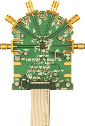
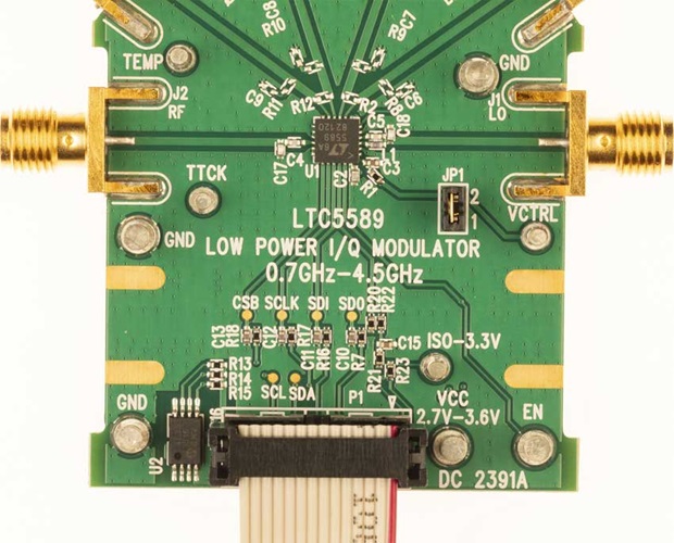
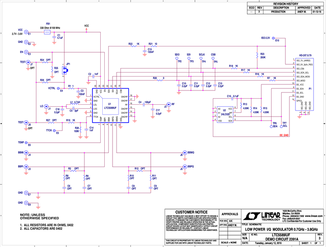
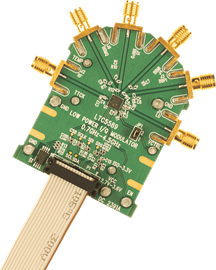
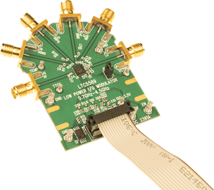
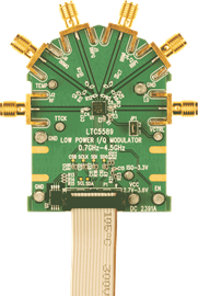
Demonstration circuit 2391A is optimized for evaluation of the LTC5589 low power I/Q modulator up to 4.5GHz. For frequencies above 4.5GHz, LO matching circuit on the DC2391A demo board can be easily modified for improved image rejection performance. Refer to data sheet for additional information. The four balanced I- and Q-baseband input ports can be either AC-coupled with internal bias supplied, or DC-coupled from a source with a common-mode voltage level of about +1.4V. The SPI interface is used to set internal registers which control the gain, optimum center frequency, I-offset, Q-offset and sideband suppression. In addition to the digital gain control with 1dB steps, there is an analog gain control, VCTRL. An on‑chip thermometer can be used to compensate for the gain vs temperature variations using a digital gain control change. The update can either be automatically triggered, or entirely switched off.
文档
-
DC2391A - Schematic2016/6/1PDF36K
-
DC2391A - Demo Manual2016/6/1PDF518K
-
DC2391A - Design Files2016/6/1ZIP1M