
Overview
Features and Benefits
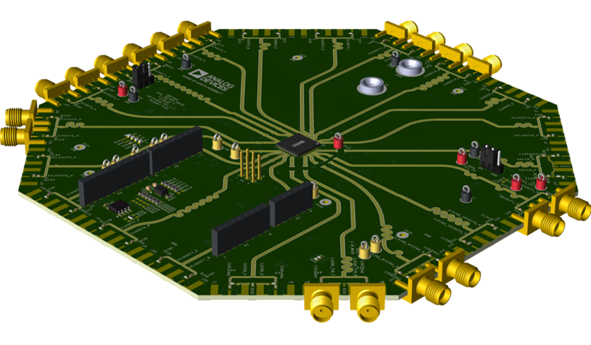
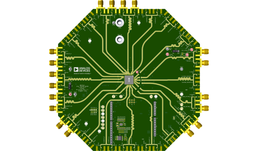
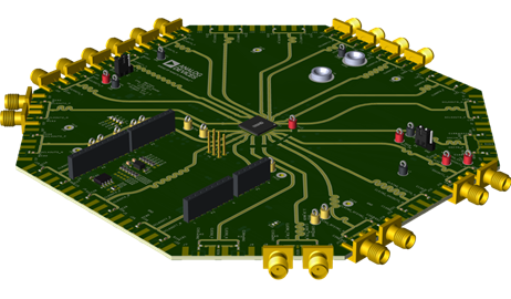
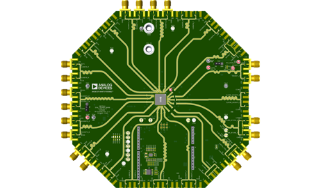
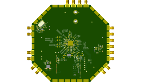
- Self-contained board, including the HMC7044B dual-loop clock jitter cleaner, loop filters, USB interface, on-board VCXO, and voltage regulators
- SMA connectors for two reference inputs, six clock outputs, and one VCXO output
- Windows®-based software allows control of synthesizer functions from a PC
- Externally powered by 6V
Product Details
This user guide describes the hardware and software of the HMC7044B evaluation kit. The evaluation board schematic and printed circuit board (PCB) layout artwork can be found on the EK1HMC7044BLP10B product page at www.analog.com.
The HMC7044B meets the requirements of multicarrier GSM and LTE base station designs, and offers a wide range of clock management and distribution features that simplify baseband and radio card clock tree designs. The high performance dual-loop core of the HMC7044B enables the base station designer to attenuate the incoming jitter of a primary system reference clock, such as a CPRI source, using the narrow-band configured first phase-locked loop (PLL), which disciplines an external voltage-controlled crystal oscillator (VCXO), and to generate the low phase noise, high frequency clocks with the wider-band second PLL to drive data converter sample clock inputs.
The EK1HMC7044BLP10B evaluation board is a compact, easy-touse platform for evaluating all the features of the HMC7044B. A 122.88MHz VCXO is mounted on the evaluation board to provide a complete solution. All inputs and outputs are configured as differential on the evaluation board. Full specifications on the HMC7044B are available in the product data sheet, which must be consulted in conjunction with this user guide when using the evaluation board.
Applicable Parts
Getting Started
EQUIPMENT NEEDED
- Windows-based PC with USB port for evaluation software
- EVAL-SDP-CK1Z (SDP-K1) controller board
- Power supply (6V)
- 50Ω terminators
- Low noise REFIN source