EVAL-ADAR4002


Overview
Features and Benefits
- Standard single-ended 50Ω interfacing
- Supply voltage easily applied to test loops or headers
- SPI signals available on the P1 and P10 headers
Product Details
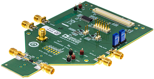
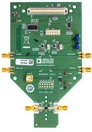
This user guide describes the ADAR4002-EVALZ evaluation board kit for the ADAR4002 0.5GHz to 19GHz, 1-channel bidirectional true time delay unit and variable attenuation device for phased array applications. The ADAR4002 features a digital stepped attenuator (DSA) block and a time delay unit (TDU) block. The TDU has two programmable time delay ranges. Range 0 offers a 508ps time delay range and 4ps step size, while Range 1 offers a 254ps time delay range and 2ps step size. See device block diagram in the ADAR4002 data sheet.
The ADAR4002-EVALZ allows the user to test all the functions and features offered by the ADAR4002 chip including variable gain, variable time delay, and both digital modes (serial peripheral interface (SPI) and shift register). RF signal traces are a 50Ω coplanar waveguide design and are connected to the RF1 port and RF2 port of the device, which provides simple interfacing with test equipment or other printed circuit boards (PCBs). The EVAL-SDP-CS1Z (SDP-S) controller board programs the SPI port or shift register using the ADAR4002 ACE plug-in.
A full description and complete specifications for the ADAR4002 are provided in the data sheet and should be consulted in conjunction with this user guide when using the ADAR4002-EVALZ evaluation board.
Applicable Parts
Getting Started
EQUIPMENT AND HARDWARE REQUIRED
- 20GHz VNA
- 2-channel power supply
- EVAL-SDP-CS1Z (SDP-S) controller board
- PC
- Digital multimeter (DMM) or voltmeter