AD9773
NOT RECOMMENDED FOR NEW DESIGNS12-Bit, 160 MSPS, 2×/4×/8× Interpolating Dual TxDAC® D/A Converter
- Part Models
- 2
- 1ku List Price
- Starting From $38.35
Part Details
- 12-bit resolution, 160 MSPS/400 MSPS input/output data rate
- Selectable 2×/4×/8× interpolating filter
- Programmable channel gain and offset adjustment
- fS/2, fS/4, fS/8 digital quadrature modulation capability
- Direct IF transmission mode for 70 MHz + IFs
- Excellent ac performance
SFDR −69 dBc @ 2 MHz to 35 MHz
WCDMA ACPR −69 dB @ IF = 19.2 MHz
- Enables image rejection architecture
- Fully compatible SPI port
- Internal PLL clock multiplier
- Selectable internal clock divider
- Versatile clock input
Differential/single-ended sine wave or TTL/CMOS/LVPECL compatible - Versatile input data interface
Twos complement/straight binary data coding
Dual-port or single-port interleaved input data
The AD9773 is the 12-bit member of the AD977x pin-compatible, high performance, programmable 2×/4×/8× interpolating TxDAC+® family. The AD977x family features a serial port interface (SPI) that provides a high level of programmability, thus allowing for enhanced system-level options. These options include selectable 2×/4×/8× interpolation filters; fS/2, fS/4, or fS/8 digital quadrature modulation with image rejection; a direct IF mode; programmable channel gain and offset control; programmable internal clock divider; straight binary or twos complement data interface; and a single-port or dual-port data interface.
The selectable 2×/4×/8× interpolation filters simplify the requirements of the reconstruction filters while simultaneously enhancing the TxDAC+ family’s pass-band noise/distortion performance. The independent channel gain and offset adjust registers allow the user to calibrate LO feedthrough and side-band suppression errors associated with analog quadrature modulators. The 6 dB of gain adjustment range can also be used to control the output power level of each DAC.
The AD9773 features the ability to perform fS/2, fS/4, and fS/8 digital modulation and image rejection when combined with an analog quadrature modulator. In this mode, the AD9773 accepts I and Q complex data (representing a single or multi-carrier waveform), generates a quadrature modulated IF signal along with its orthogonal representation via its dual DACs, and presents these two reconstructed orthogonal IF carriers to an analog quadrature modulator to complete the image rejection upconversion process. Another digital modulation mode (for example, the direct IF mode) allows the original baseband signal representation to be frequency translated such that pairs of images fall at multiples of one-half the DAC update rate.
Dual high performance DAC outputs provide a differential current output programmable over a 2 mA to 20 mA range. The AD9773 is manufactured on an advanced 0.35 micron CMOS process, operates from a single supply of 3.1 V to 3.5 V, and consumes 1.2 W of power.
PRODUCT HIGHLIGHTS
- The AD9773 is the 12-bit member of the AD977x pin compatible, high performance, programmable 2×/4×/8× interpolating TxDAC+ family.
- Direct IF transmission is possible for 70 MHz + IFs through a novel digital mixing process.
- fS/2, fS/4, and fS/8 digital quadrature modulation and user selectable image rejection simplify/remove cascaded SAW filter stages.
- A 2×/4×/8× user selectable interpolating filter eases data rate and output signal reconstruction filter requirements.
- User selectable twos complement/straight binary data coding.
- User programmable channel gain control over 1 dB range in 0.01 dB increments.
- User programmable channel offset control ±10% over the FSR.
- Ultrahigh speed 400 MSPS DAC conversion rate.
- Internal clock divider provides data rate clock for easy interfacing.
- Flexible clock input with single-ended or differential input, CMOS, or 1 V p-p LO sine wave input capability.
- Low power: Complete CMOS DAC operates on 1.2 W from a 3.1 V to 3.5 V single supply. The 20 mA full-scale current can be reduced for lower power operation, and several sleep functions reduce power during idle periods.
- On-chip voltage reference: The AD9773 includes a 1.20 V temperature compensated band gap voltage reference.
- 80-lead thin quad flat package, exposed pad (TQFP_EP).
Documentation
Data Sheet 1
Application Note 7
Solutions Bulletin & Brochure 1
ADI has always placed the highest emphasis on delivering products that meet the maximum levels of quality and reliability. We achieve this by incorporating quality and reliability checks in every scope of product and process design, and in the manufacturing process as well. "Zero defects" for shipped products is always our goal. View our quality and reliability program and certifications for more information.
| Part Model | Pin/Package Drawing | Documentation | CAD Symbols, Footprints, and 3D Models |
|---|---|---|---|
| AD9773BSVZ | 80 ld TQFP with exposed pad | ||
| AD9773BSVZRL | 80 ld TQFP with exposed pad |
| Part Models | Product Lifecycle | PCN |
|---|---|---|
|
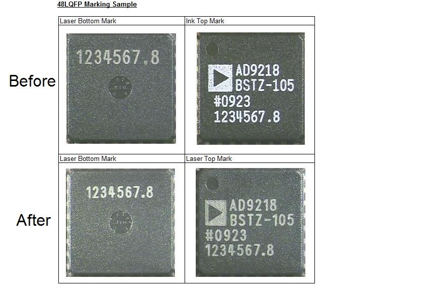
Jun 16, 2009 - 09_0027 Conversion to Laser Mark for the LQFP Packages (Single Grades) |
||
| AD9773BSVZ | PRODUCTION | |
| AD9773BSVZRL | PRODUCTION | |
This is the most up-to-date revision of the Data Sheet.
Software Resources
Can't find the software or driver you need?
Request a Driver/SoftwareHardware Ecosystem
| Parts | Product Life Cycle | Description |
|---|---|---|
| AD9125 | RECOMMENDED FOR NEW DESIGNS | Dual, 16-Bit, 1000 MSPS, TxDAC+® Digital-to-Analog Converter |