A Wideband Analog Front End Based on a Continuous Time, ∆-Σ High Speed ADC Reduces Power Consumption of High Performance Communication and Instrumentation Systems
A Wideband Analog Front End Based on a Continuous Time, ∆-Σ High Speed ADC Reduces Power Consumption of High Performance Communication and Instrumentation Systems
2015年03月01日
Continuous time ∆-Σ (CTDS) analog-to-digital converters (ADCs) are the architecture of choice for audio systems, phone handsets, and mobile electronics. This ADC architecture allows efficient integration, signal chain reduction, and low power consumption, among other benefits. While CTDS ADCs outperform other classes of ADCs when high dynamic range and power efficiency are the primary requirements, other types of ADCs, such as pipelined ADCs, have been the mainstream choice for cellular communication infrastructure systems, thanks to their ability to convert wideband analog input signals.
Recent technology breakthroughs introduced at Analog Devices are now allowing CTDS ADCs to digitize wideband signals at very high frequencies. This overcomes previous limitations and also enables the significant system level benefits in wider band systems introduced by CTDS ADCs that made them pervasive in lower frequency applications.
This article describes the implementation of such recent innovations. In particular an analog front end, including a wideband CTDS bandpass ADC at its core, for the digitization and downconversion of high frequency signals in communication and instrumentation systems is discussed. The embedded band-pass ADC does not require an external antialiasing filter and driving amplifiers/buffers, substantially reducing the signal chain’s component count, power consumption, and relaxing its overall specifications. Moreover on-chip programmable digital filtering and downconversion are also integrated, providing a complete and easy to use solution to the designer.
Continuous time ∆-Σ (CTDS) ADCs1 have been the analog-to-digital architecture of choice in a broad set of applications ranging from high performance audio to cellular handset RF front ends for several years owing to a number of advantages over other types of ADCs. The benefits include greater amenability to integration and low power consumption, but also, and possibly more importantly, because using a CTDS solves a number of significant system level problems. Due to a number of technology shortcomings, the use of CTDS has been previously limited to relatively lower frequency/bandwidth and lower dynamic range. Therefore, high performance Nyquist rate converters, such as pipelined and successive approximation ADCs, have been the mainstream solution for high performance/high frequency digitization applications.
However, recent technology breakthroughs introduced at Analog Devices have allowed overcoming many prior limitations. Hence, making high speed ADCs based on CTDS able to achieve substantially higher performance specifications, stability in the presence of strong interferers, programmable frequency response, and in turn, enabling the solution of a number of important signal processing problems in cellular infrastructure systems and selected high performance instrumentation applications among others.
To better understand that, let us consider, a classic heterodyne receive signal chain for a communication system. A traditional scheme using a mainstream switched capacitor Nyquist rate, high speed ADC is depicted in Figure 1(a). Here, the intermediate frequency (IF) signal produced by the mixer needs to be buffered and possibly amplified using a driving amplifier. The Nyquist ADC also requires an antialiasing filter (AAF), sometimes implemented by a surface acoustic wave (SAW) filter or a multipole discrete SMD filter. Finally, the desired IF radio signal reaches the ADC. Its output, clocked at a high sample rate fs (with fs/2 substantially larger than the center/IF frequency), is further processed (filtered and downconverted to baseband) by a communication digital ASIC.

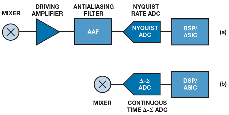
The same processing chain dramatically simplifies when using a CTDS as shown in Figure 1(b). Since the CTDS has a resistive input, it can be driven directly by the mixer and does not require a driving amplifier. Moreover, the CTDS’s inner core includes a CT analog filter which implicitly performs the AAF function and hence allows doing away2 with the input SAW/SMD discrete filter. Furthermore, the CTDS can have a band-pass filter frequency characteristic (see Figure 2 for an example of actual measurements), tunable to center at the desired IF input frequency, and with a significant out-of-band attenuation. Such pass band is oversampled, digitized, and it is digitally decimated and downconverted to baseband and provided to the digital ASIC at a much lower data rate (and with lower power consumption) than in the case of Figure 1(a).


The above described system level simplification is the direct result of fundamental architectural differences between CTDS and other high speed ADC architectures.
The additional benefits of this simplification are substantial. In Figure 1(a), the driving amplifier can consume a comparable power as the ADC itself while impacting the overall noise figure of the chain. The AAF in Figure 1(a) cannot be easily integrated. Moreover, a new filter needs to be suitably selected for each choice of IF (and frequency plan) and specific signal chain implementation. Experienced system designers know that the implementation of the filter can often be very time consuming as different component selections with the same filter function can lead to dramatically different linearity performance due to the nonlinear interaction with the front-end sampling circuitry of the Nyquist ADC. Conversely, in Figure 1(b), where the AAF filter is removed and a front-end sampling circuitry is replaced by the CTDS’s benign resistive input, the filtering function is performed by the CTDS and its frequency characteristic has been made digitally programmable in Analog Devices’ technology. Therefore, the very same CTDS can be interchangeably used in multiple signal chains and digitally tuned to the desired frequency and bandwidth, greatly simplifying and accelerating the overall platform development process as well. Needless to say, for equal function and performance, the signal chain in Figure 1(b) has both lower power consumption and smaller form factor than the one in Figure 1(a).
An instantiation of this technology can be found in Analog Devices’ AD6676 with functional block diagram shown in Figure 3. The latter is an integrated IF digitization subsystem embedding a tunable band-pass CTDS with very high instantaneous dynamic range along with digital filtering and downconversion functions, automatic gain control support, integrated clock synthesizer, and a JESD204B serial output interface. The center frequency (IF) of the pass band can be digitally tuned between 70 MHz and 450 MHz, and its bandwidth can be programmed to be between 20 MHz and 160 MHz with varying in-band noise spectral density.

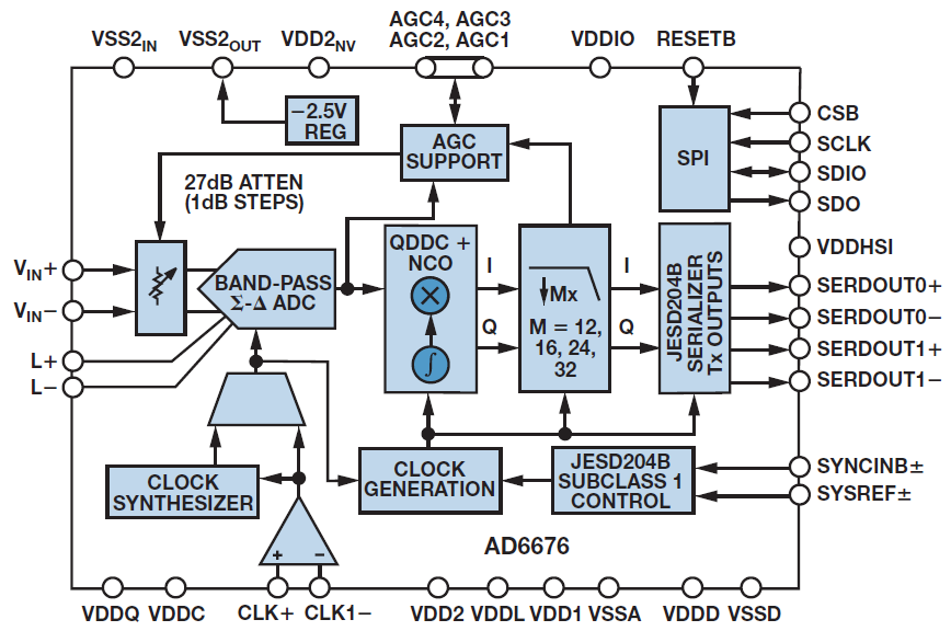
The performance of this part, as found in its data sheet, makes it suitable for a variety of wideband cellular infrastructure equipment and repeaters, point-to-point microwave equipment, spectrum analyzers, communication instrumentation, and many other functions.
Conclusion
Important signal chain simplification and performance optimization, and increased system design flexibility and reduction in its development effort can be realized when continuous time ∆-Σ ADCs are used. Some of the benefits of these architectures have previously made them common in a variety of low power and mobile applications. Thanks to a number of recent IC technology breakthroughs, CTDS is now also able to meet the stringent ADC high dynamic performance requirements of many communication infrastructure and instrumentation systems while maintaining stable operation in the presence of strong in-band and out-of-band interferers. An IF subsystem embedding a band-pass CTDS high speed converter with programmable center frequency (IF) and bandwidth combined with a digital downconversion and filtering postprocessing back-end stage, along with other integrated functions, provides a very flexible and powerful solution for software radio applications. Moreover, it also results in overall system level reduction, increased flexibility, and performance optimization of the signal chain by further allowing elimination of a number of additional signal conditioning blocks otherwise mandated by mainstream ADC technology.
著者について
Gabriele Manganaroは、イタリアのカターニア大学で電子工学の博士号を取得しています。1994年にSTMicroelectronics社とテキサスA&M大学で研究を始めました。Texas Instruments社、Engim社、National
この記事に関して
製品


