Voltage Margining Made Easy
Introduction
Analog Devices has introduced two devices that simplify supply margin testing and are particularly well suited for multiple power supply applications. The LTC2920-1 is a single power supply margining controller packaged in a 5-lead SOT-23. The LTC2920-2 is a dual power supply margining controller packaged in an 8-lead MSOP. Both parts provide an easy and accurate way to accomplish onboard power supply margining with a minimum of design time and board space.
What is Voltage Margining?
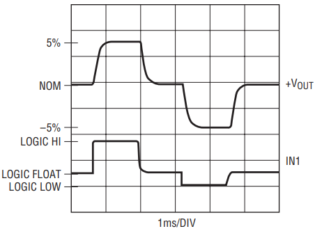
High performance and high reliability systems typically require end-of-line testing, or include automated self-testing, to assure rated performance with the supply voltage at the upper and lower limits of its regulation band. This testing is often called “supply margining” or “voltage margining.” The testing is typically accomplished by forcing the power supply modules or DC/DC converters in the system to ±5% of their nominal voltage. Once the supply voltage has settled at the margined voltage, the system performance can be evaluated. Figure 1 shows typical rise and fall times for voltage margining waveforms.

Figure 1. Typical voltage margining waveforms
Typical Applications
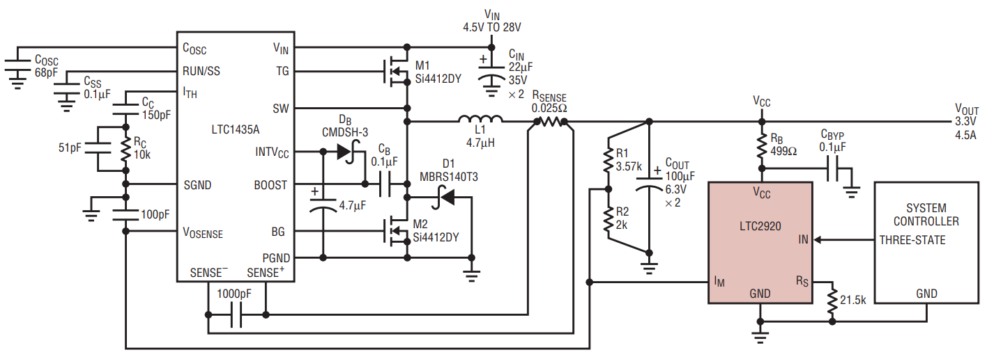
Figure 2 shows how the 5-lead SOT23 LTC2920-1 controls a LTC1435A switching regulator by sourcing or sinking current at the feedback pin. This margining solution takes fewer components, less board space, and less design time than the traditional approach of using resistors, switches, and level shifters. Figure 3 shows the LTC2920-1 controlling a DC/DC converter module. In this case, current is forced into or out of the trim pin on the module, causing it to raise or lower its output voltage accordingly.

Figure 2. Voltage margining a switching power supply.
Easy to Use, Easy to Connect
The LTC2920-1 uses only three pins to setup and control the margining of a power supply: the IM current pin, the current selecting pin RS, and the control pin IN. The feedback node or trim pin of the power supply to be margined is connected to the IM pin. The margining current is selected with a single resistor, RSET, connected to the RS pin. The RSET resistor can program the margin current over a 400:1 range from 5µA to 2mA. The control input is a three-state signal: LOW to margin down, HIGH to margin UP, and FLOAT to allow the power supply to regulate at its nominal voltage. The only other pins are power and ground. The LTC2920-2 has an additional independent margining channel, adding a second set of IM, RS, and IN pins.

Figure 3. DC to DC converter voltage margining
The LTC2920-1 uses less than 14mm2 of application board space, and the LTC2920-2 uses less than 27mm2 (Figure 4). These numbers include the current setting resistors and the LTC2920’s power supply bypass capacitor.

Figure 4. Dual power supply voltage margin controller occupies less than 27mm2
How It Works
Feedback Circuits
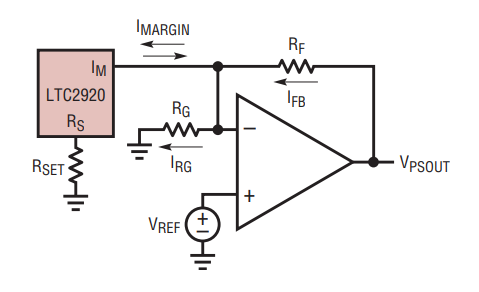
The LTC2920 provides symmetric power supply margining by taking advantage of the architecture common to most power supplies. Most regulated power supplies rely on feedback and gain to maintain power supply output voltages. Even complicated multi-phase switching power supplies can typically be modeled as a simple amplifier with a voltage reference and two feedback resistors (Figure 5). The LTC2920 creates a delta voltage across the feedback resistor RF by sourcing or sinking current from the feedback node. Here’s how it works:

Figure 5. Simplified power supply model
Knowing the value of the resistors RF and RG, and the voltage of VREF, VPSOUT can be calculated from the basic op amp feedback equation:

Since the op amp keeps its inverting terminal equal to the noninverting terminal, the voltage at the inverting terminal between RF and RG is VREF. There is no significant current flowing into or out of the op amp inputs, so:

Knowing that this current flows in the feedback resistor network, VPSOUT can be alternately calculated by:

This equation is in a form which is helpful for understanding how the LTC2920 changes the power supply output voltage. Figure 6 shows the simplified model with the LTC2920 added. As before, the op amp keeps the voltage at its inverting input at VREF. If we add or subtract current at this node, the delta current is always added to or subtracted from IFB, and never IRG. Because of this, the voltage across RF is:

Figure 6. Simplified power supply model with voltage margining

When added to the nominal voltage at the feedback pin VREF, the power supply output becomes:

This is the nominal power supply output voltage, plus or minus the margining current, IMARGIN, supplied by the LTC2920 times the feedback resistor RF:

Note that the delta voltage VMARGIN depends only on IMARGIN and RF, and not RG or VREF.
Simple Design: Calculate the Value of One Resistor
There is one resistor value to calculate when designing in the LTC2920 for voltage margining applications: the current setting resistor RSET. To calculate this value, there are only two things the designer needs to know: the amount of voltage to margin the power supply, VMARGIN, and the value of the feedback resistor of the margined power supply, RF.
The value of the current setting resistor can then be determined by calculating the desired IMARGIN current sourced or sunk by the LTC2920:

The value of the current setting resistor is then:

And in its simplest form:

No Access to the Feedback Pin? No Problem
DC to DC power supply modules typically do not provide access to the feedback pin directly, but DC to DC power modules often have a trim pin. In this application, the LTC2920 operates by sourcing and sinking current out of the trim pin on the power supply being margined. Calculation of the RSET resistor is slightly more complicated than the case described above, requiring a bench measurement to be made on the DC to DC power supply module. See the LTC2920 data sheet for details on the operational details and how to calculate the RSET resistor.
Conclusion
The LTC2920-1 and LTC2920-2 Power Supply Margining Controllers provide a cost effective way to add self-testing capability to high performance and high reliability systems. They are easy to design with easy to interface to. Both parts have the ability to control power supplies with either feed back nodes, or trim pins. With printed circuit footprints of less than 14mm2 and 27mm2, the LTC2920-1 and LTC2920-2 respectively provide versatile power supply margining with a minimum impact on PCB space.


