Ultralow Power 14-Bit Serial ADC Samples at 400ksps
Introduction
The LTC1417 is a new and versatile 14-bit ADC that samples at up to 400ksps while consuming just 20mW from a single 5V supply. The LTC1417 is designed to be adaptable and easy to use, requiring little or no support circuitry in a wide variety of applications. Some of the key features of this new device include:
- 400ksps throughput
- 82dB SINAD and –95dB THD at Nyquist
- Low power—20mW
- Single 5V or ±5V supplies
- 1.25LSB INL max and 1LSB DNL max
- Differential inputs
- Serial data output
- NAP and SLEEP power shutdown modes
- Small package—16-pin SSOP
High Performance with Low Power
Figure 1 shows a block diagram of the LTC1417. This device includes a high performance differential sample-and-hold circuit, an ultra-efficient successive-approximation ADC, an on-chip reference and a serial digital interface that easily interfaces to microprocessors, FIFOs or DSPs. The LTC1417 is factory calibrated, so a lengthy calibration cycle is not required to achieve 14-bit performance. DC specifications include a 1LSB (max) differential linearity error (no missing codes) and ±1.25LSB max integral linearity error, both guaranteed over temperature. Typical INL and DNL curves are shown in Figures 2a and 2b. The gain of the ADC is controlled by an on-chip 10ppm/°C reference that can be easily overdriven with an external reference if required.
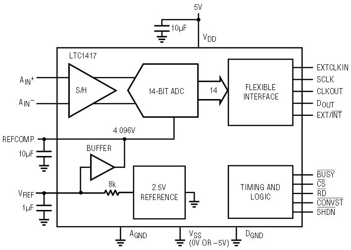
Figure 1. LTC1417 block diagram.
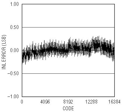
Figure 2a. The LTC1417’s typical INL is less than ±0.5LSB.

Figure 2b. With a typical DNL of less than ±0.35LSB, the LTC1417 is a true 14-bit-accurate part.
For AC applications, the dynamic performance of the LTC1417 is exceptional. The extremely low distortion differential sample-and-hold has a typical full-power bandwidth of 10MHz. The spurious free dynamic range is typically 95dB at the 200kHz Nyquist frequency. The part’s low noise and low distortion achieve a signal-to-noise ratio (SNR) of 82dB from DC to well beyond Nyquist. Figure 3 shows the typical SINAD and ENOB versus input frequency. The FFT in Figure 4 shows the that the typical THD is composed of second and third harmonics; the higher harmonics are below the noise floor. Figure 5 shows the second and third harmonic distortion versus input frequency.

Figure 3. With a SINAD of 82dB, the LTC1417 maintains 13.4ENOB at the 200kHz Nyquist frequency.
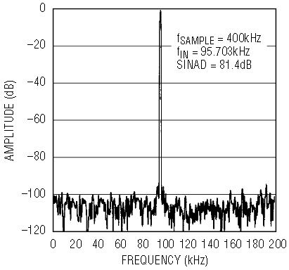
Figure 4. The LTC1417’s linearity, as shown in this FFT, helps preserve signal integrity while allowing only small amounts of second and third harmonic distortion. Any remaining distortion is below the part’s noise floor.
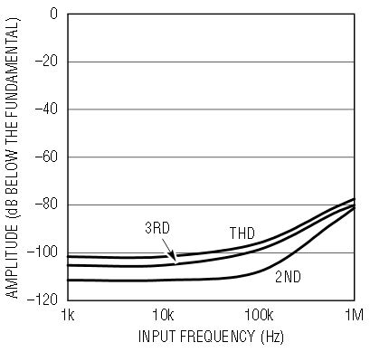
Figure 5. As the input signal’s frequency increases, second and third harmonic distortion remain low.
The LTC1417’s superior AC and DC performance doesn’t require a lot of power. In fact, the LTC1417 is one of the lowest power 14-bit ADCs available, dissipating just 20mW at 400ksps (10mW at sample rates below 125ksps). Two shutdown modes make it possible to decrease power consumption even further as the sampling rate is reduced. This will be described in greater detail later in this article.
High Impedance Inputs
The LTC1417’s high impedance inputs allow direct connection of high impedance sources without introducing errors. Many ADCs have a resistive input or input bias current that requires a low source impedance to achieve low errors. Often, ADCs with switched capacitor inputs exhibit large offset shifts when driven with a high source impedance or a large source-impedance imbalance between their differential inputs. The LTC1417’s unique sample-and-hold circuit has a low capacitance, high resistance (10MΩ ||14pF) switched capacitor input that has only 4.5LSB of offset shift with a source impedance imbalance between 0Ω and 1MΩ (see Figure 6a). (There is no shift if +AIN and –AIN see equal source impedances.) Connecting the ADC directly to a high impedance source avoids the additional noise and offset errors that may be introduced by buffering circuitry. The only downside caused by directly connecting the ADC to a high source impedance is increased acquisition time. However, because of the LTC1417’s low input capacitance (14pF), the ADC achieves full-speed operation while operating with source impedances up to 2kΩ. Above 3kΩ, the sample rate must be reduced, as shown in Figure 6b.

Figure 6a. Change in offset voltage with source resistance mismatch.
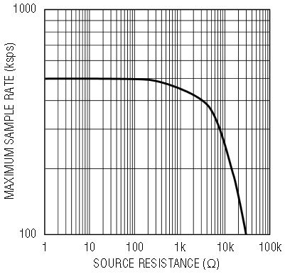
Figure 6b. Maximum sample rate vs unbuffered source resistance.
Differential Inputs with Wideband CMRR
Another benefit of the LTC1417’s differential input is excellent common mode rejection, which eliminates the need for most input-conditioning circuitry. Op amps and instrumentation amplifiers are often used to reject common mode noise from EMI, AC power and switching noise. Although these circuits perform well at low frequencies, their rejection at high frequencies deteriorates substantially. Figure 7 shows how the LTC1417’s CMRR remains strong as the frequency increases.
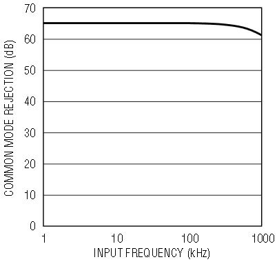
Figure 7. Input common mode rejection vs input frequency.
Single- or Dual-Supply Operation
Single-supply ADCs can be cumbersome to use in a dual-supply system. A signal with a common mode of zero volts has to be shifted to the ADC’s common mode voltage. Shifting the common mode can be accomplished with AC coupling, but DC information is lost. Alternatively, an op amp level shifter can be used, but this adds circuit complexity and additional errors. The LTC1417 overcomes these limitations because it operates with single or dual supplies, which allows input signals to be direct coupled in both cases. With a single supply, VSS = 0V and the ADC operates in unipolar mode with an input range of 0V to 4.096V. The ADC is equipped with circuitry that automatically detects when –5V is present on the VSS pin. With a –5V supply, the ADC operates in bipolar mode and the full-scale range becomes ±2.048V for +AIN with respect to –AIN.
On-Chip Reference
The LTC1417’s on-chip reference is a standard 2.5V and is available on the VREF output (pin 3). An internal amplifier increases the reference’s 2.5V to 4.096V, setting the ADC’s full-scale span. The 4.096V output is available on the REFCOMP output (pin 4) and may be used as a reference for other external circuitry. With a temperature coefficient of 10ppm/°C, both VREF and REFCOMP are well suited to function as a system’s master reference. However, if an external reference circuit is required, it can easily overdrive either reference output. The 2.5V reference output is resistive (8k) and can be easily overdriven by any reference with low output impedance by directly connecting the external reference to the REF pin. When overdriving the REFCOMP (the 4.096V reference) output, tie the VREF pin to ground. This disables the output drive of the REFCOMP amplifier, allowing it to be easily overdriven.
Simple, Versatile Serial Interface
While simple, the LTC1417’s four-mode serial interface does not sacrifice flexibility. Serial data can be clocked with the internal shift clock for minimal hardware or with an external shift clock for synchronization. Additionally, data can be clocked out during the conversion for the highest throughput rate or after the conversion for maximum noise immunity. Its simplest mode uses just three pins for data transfer: a data-out pin, a serial clock pin and a control pin. With more connections, the conversion and the output data can be clocked at different rates, optimized for a given controller or processor and application.
Figure 8 shows a simple, basic 4-wire connection between a host processor and the LTC1417. This interface consists of a convert-start signal, serial shift clock, serial data and an end-of-conversion signal. The conversion is started by applying a logic low to the LTC1417’s CONVST pin. The conversion is completed using the internal clock. This same clock is present on the CLKOUT pin and is used by the processor to latch the data that is generated and read during the conversion. The BUSY output changes to a logic low at the start of conversion, remains low during conversion, framing the data, and returns to a logic high at the end of conversion.

Figure 8. This simple 4-wire connection uses the LTC1417’s internal clock to simultaneously clock the conversion and shift out the data.
Figure 9 shows a more complex, but more versatile, interface. This configuration uses the LTC1417’s internal clock to step through the conversion and an externally supplied clock to retrieve the data after the conversion’s completion. This configuration allows the ADC to complete the conversion and store the data in the background, after which the processor, when it is ready, asserts RD and retrieves the data.
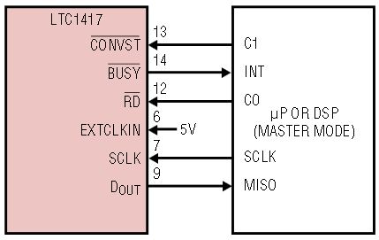
Figure 9. This connection uses the LTC1417’s internal clock to clock the conversion. The data is held internally until the processor asserts RD, applies an external clock and retrieves the data.
Perfect for Telecom: Wide Dynamic Range
With its low noise and low distortion, the LTC1417 offers extremely wide dynamic range over its entire Nyquist bandwidth. This benefit is essential to applications such as telecommunications systems. Spurious free dynamic range is typically 95dB and only starts to drop off at input frequencies above Nyquist. The ultralow 5psRMS jitter of the sample-and-hold keeps the SNR flat from DC to 1MHz, making this device useful for undersampling applications.
Another important requirement for telecom systems is a low error rate. In any ADC, there is a finite probability that a large conversion error (greater than 1% of full scale) will occur. In video or flash converters, these large errors are called “sparkle codes.” Large errors are a problem in telecom systems such as ISDN, because they result in data-transmission errors. All ADCs have a rate at which errors occur, referred to as the error rate. The error rate is dependent on the ADC architecture, design and process. Error rates vary greatly and can be as low as one in ten billion to as high as one in one million. Telecom systems typically require error rates to be one in one billion or better.
A benefit of the LTC1417’s design is ultralow error rates. The error rate is so low that it is difficult to measure because of the time between errors. To make measurement more practical, the error rate was measured at an elevated temperature of 150°C, because error rate increases with temperature. Even at this high temperature, the error rate was one in 100 billion. The projected error rate at room temperature is one in 2,000,000 billion or about one error every 158 years if running at the full conversion rate.
Ideal for Low Power Applications
LTC1417 is especially well suited for applications that require low power and high speed. The normal operating power is low—only 20mW. Power may be further reduced if there are extended periods of time between conversions. During these inactive periods when the ADC is not converting, the LTC1417 may be shut down. There are two power shutdown modes: NAP and SLEEP.
NAP mode shuts down 85% of the power and leaves only the reference and logic powered. The LTC1417 can wake up from NAP mode very quickly; in just 500ns it can be ready to start converting. In NAP mode, all data-output control is functional; data from the last conversion prior to starting NAP mode can be read during NAP mode. RD controls the state of the output buffers. NAP mode is useful for applications that must be ready to immediately take data after long inactive periods.
With slow sample rates, power can be saved by automatically invoking NAP mode between conversions. Referring to Figure 10, the SHDN and CONVST pins are driven together. A conversion will be started with the falling edge of this signal; once the conversion is completed, the ADC will automatically shut down. Before the next conversion can start, the CONVST and SHDN pins must be brought high early enough to allow for the 500ns wake-up time. Power drops with the sample frequency until it approaches the power of the reference circuit, about 2mW at frequencies less than 10kHz.
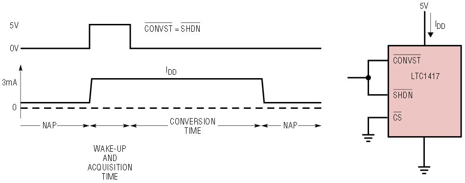
Figure 10. NAP mode between conversions.
The SLEEP mode is used when the NAP-mode current drain is too high or if wake-up time is not critical. In SLEEP mode, all bias currents are shut down, the reference is shut down and the logic outputs are put in a high impedance state. The only current that remains is junction leakage current, less than 1µA. Wake-up from the SLEEP mode is much slower, since the reference circuit must power up and settle to 0.01% for full accuracy. The wake-up time is also dependent on the value of the compensation capacitor used on the REFCOMP pin; with the recommended 10µF capacitor, the wake-up time is 10ms. SLEEP mode is useful for long inactive periods, that is, times greater than 10ms.
Layout Considerations
As with other high resolution, high speed ADCs, the LTC1417 needs some basic attention to layout details. These include grounding, bypassing and lead inductance. The best performance is achieved when the LTC1417 is treated as an analog part, powered by an analog supply and grounded to an analog ground plane through its DGND and AGND pins. The analog and digital ground planes should be connected at only one of two places, the LTC1417’s DGND pin or a PCB’s ground input. Elsewhere, the analog ground plane should never underlie or touch the digital ground plane. To ensure minimum inductance and best performance, the analog ground plane can be overlaid by analog supply traces or the power plane that feeds the LTC1417 5V or ±5V power. Figure 11 shows some suggestions for proper layout, bypassing and connections for an op amp when needed.
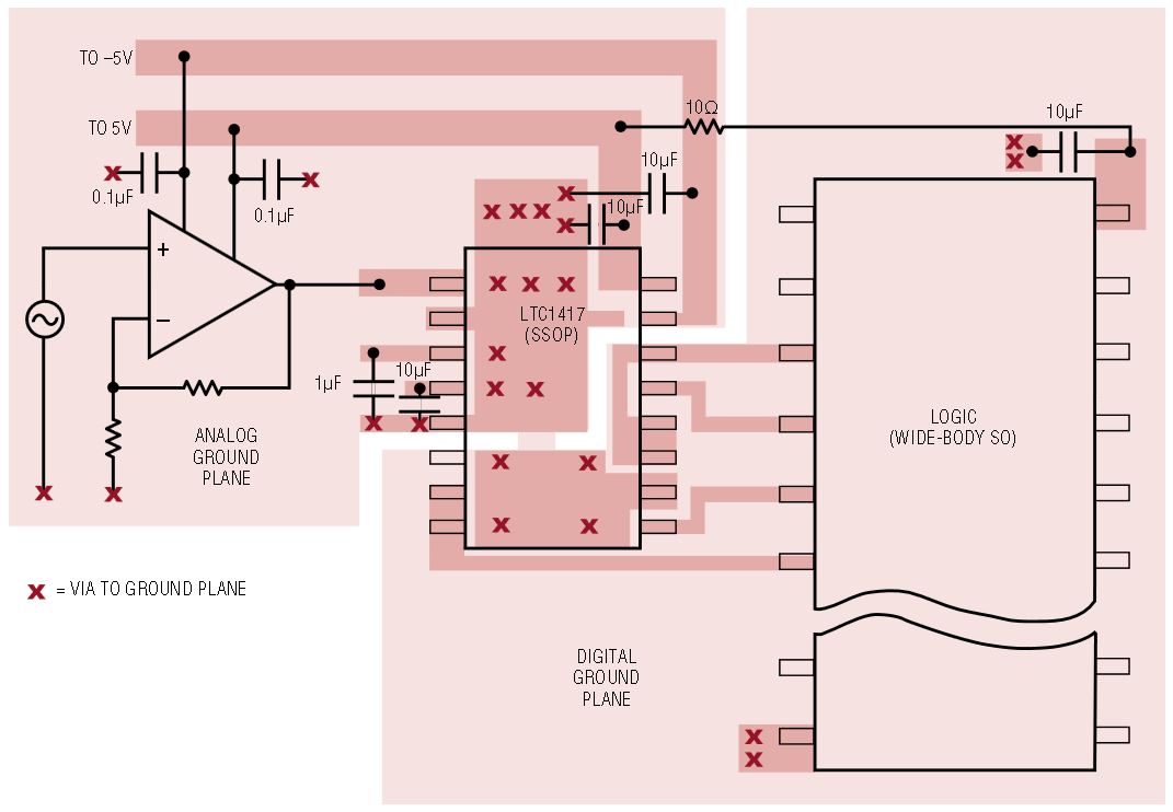
Figure 11. This suggested layout, with analog and digital ground planes, closely positioned bypass components and multiple ground connections between the ADC’s ground pin and the ground planes, maximizes the LTC1417’s AC performance.
There are some important points to remember to achieve the best performance from the LTC1417. Use 10µF (1µF for VREF) surface mount ceramic capacitors with the shortest and widest possible traces to bypass the supply, VREF and VREFCOMP pins. Maximizing trace area reduces inductance and maximizes bypass capacitor performance. Power, reference and ground traces should also be as wide as possible.
Conclusion
The new LTC1417 low power, 14-bit ADC will find uses in many types of applications, from industrial instrumentation to telephony. The LTC1417’s adaptable analog input and serial output reduce the need for expensive support circuitry. This can result in a smaller, lower cost system.


