Small 1.25A Step-Down Regulator Switches at 4MHz for Space-Sensitive Applications
Small 1.25A Step-Down Regulator Switches at 4MHz for Space-Sensitive Applications
著者
Damon Lee
2002年05月01日
Introduction
Cell phones, pagers, PDAs and other portable devices are shrinking, and as they shrink, the demand for smaller components grows. The ubiquitous switching regulator, which solves the problem of creating a constant voltage from inconstant batteries, is not exempt from the demand to become smaller. One way to shrink regulator circuitry is to increase the switching frequency of the regulator, allowing the use of smaller and less costly capacitors and inductors to complete the circuit. Another way is to shrink the switcher itself by putting the switcher and MOSFETs in a small monolithic package. The LTC3411 DC/DC converter does both.
The LTC3411 is a 10-lead MSOP, synchronous, step-down, current mode, DC/DC converter, intended for medium power applications. It operates within a 2.5V to 5.5V input voltage range and switches at up to 4MHz, making it possible to use tiny capacitors and inductors that are under 2mm in height. By using the LTC3411 in a small MS10 package, a complete DC/DC converter can consume less than 0.3 square inches of board real estate, as shown in Figure 1.

Figure 1. A complete DC/DC converter can take less than 0.3in2 of board space
The output of the LTC3411 is adjustable from 0.8V to 5V. For battery-powered applications that have input voltages above and below the output, the LTC3411 can also be used in a single inductor, positive Buck-Boost converter configuration. A built-in 0.11Ω switch allows up to 1.25A of output current at high efficiency. OPTI-LOOP® compensation allows the transient response to be optimized over a wide range of loads and output capacitors.
Efficiency takes on grave importance in battery-powered applications, and the LTC3411 keeps efficiency high. Automatic, power saving Burst Mode® operation reduces gate charge losses at low load currents. With no load, the converter draws only 62µA, and in shutdown, it draws less than 1µA, making it ideal for low current applications.
The LTC3411 uses a current mode, constant frequency architecture that benefits noise sensitive applications. Burst Mode operation is an efficient solution for low load current applications, but sometimes noise suppression takes on more importance than efficiency, especially in telecommunication devices. To reduce noise problems, the LTC3411 provides a pulse-skipping mode and a forced-continuous mode. These modes decrease the ripple noise and improve noise filterability. Although not as efficient as Burst Mode operation at low load currents, pulse-skipping mode and forced continuous mode can still provide high efficiency for moderate loads (see Figure 3). In dropout, the internal P-channel MOSFET switch is turned on continuously, thereby maximizing the usable battery life.
A High Efficiency 2.5V Step-Down DC/DC Converter with all Ceramic Capacitors
The low cost and low ESR of ceramic capacitors make them a very attractive choice for use in switching regulators. Unfortunately, the ESR is so low that it can cause loop stability problems. Solid tantalum capacitor ESR generates a loop zero at 5KHz to 50KHz that is instrumental in giving acceptable loop phase margin. Ceramic capacitors remain capacitive to beyond 300KHz and usually resonate with their ESL before ESR becomes effective. Also, ceramic caps are prone to temperature effects, requiring the designer to check loop stability over the operating temperature range. For these reasons, great care must be taken when using only ceramic input and output capacitors. The LTC3411 helps solve loop stability problems with its OPTI-LOOP phase compensation adjustment, allowing the use of ceramic capacitors. For details, and a process for optimizing compensation components, see Linear Technology Application Note 76.
A typical application for the LTC3411 is a 2.5V step-down converter using only ceramic capacitors, as shown in Figure 2. This circuit provides a regulated 2.5V output, at up to 1.25A, from a 2.5V to 5.5V input. Efficiency for the circuit is as high as 95% for a 3.3V input as shown in Figure 3.

Figure 2. Step-down 2.5V/1.25A regulator
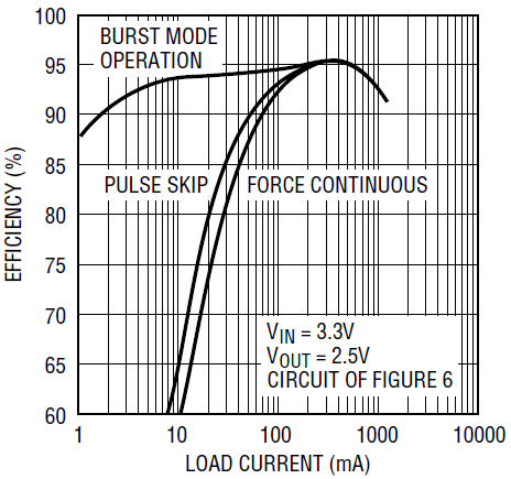
Figure 3. Efficiencies for the circuit shown in Figure 2, under different operating modes
Although the LTC3411 is capable of operating at 4MHz, the frequency in this application is set for 1MHz by R4 to improve the efficiency. Also, the availability of capacitors and inductors capable of 4MHz operation is limited.
Figures 3 through 6 show the trade-off between noise and efficiency for the different modes for the circuit. Figure 3 shows the efficiencies, while Figures 4, 5 and 6 show the output voltage and inductor current for different operating modes.
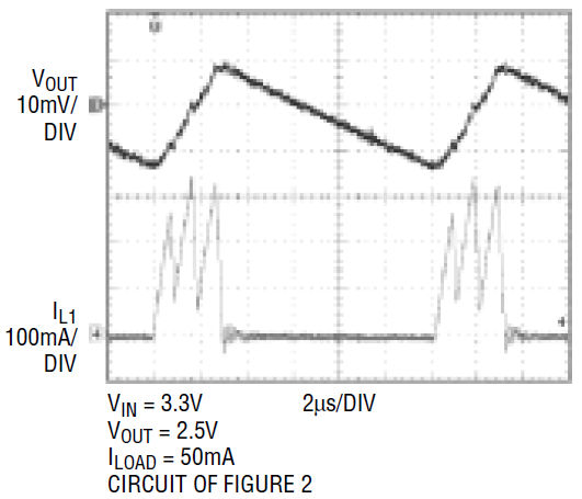
Figure 4. Burst Mode operation
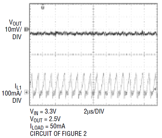
Figure 5. Pulse skipping mode
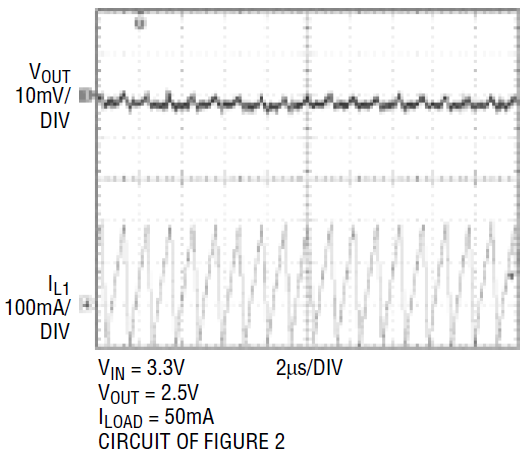
Figure 6. Forced continuous mode
Burst Mode operation is the most efficient for low current loads, but it is also generates the most complicated noise patterns. Figure 4 shows how Burst Mode operation produces a single pulse or a group of pulses that are repeated periodically. By running cycles in periodic bursts, the switching losses—dominated by the gate charge losses of the power MOSFET—are minimized. Figure 5 shows how in pulse skipping mode, the LTC3411 continues to switch at a constant frequency down to very low currents, minimizing the ripple voltage and ripple current. Finally, Figure 6 shows how in forced continuous mode, the inductor current is continuously cycled, creating a constant ripple at all output currents. Forced continuous mode is particularly useful in noise-sensitive telecom applications since the constant frequency noise is easy to filter. Another advantage of this mode is that the regulator is capable of both sourcing and sinking current into a load. This mode is enabled by forcing the mode pin to half of VIN.
Single Cell Li-Ion to 3.3V DC/DC Converter
Lithium-Ion batteries are popular in many portable applications because of their light weight and high energy density, but the battery voltage ranges from a fully charged 4.2V down to a drained 2.5V. When a device requires a voltage output that falls somewhere the middle of the Li-Ion operating range, say 3.3V, a simple buck or boost converter does not work. One solution is a single inductor, positive buck-boost converter, which allows the input voltage to vary above and below the output voltage.
In Figure 7, the LTC3411 is used in a single Inductor, positive buck-boost configuration to supply a constant 3.3V with 400–600mA of load current, depending on the battery voltage. This circuit is well suited to portable applications because none of the components exceed 3mm in height.
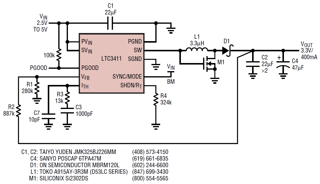
Figure 7a. Single inductor, positive, buck-boost converter
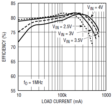
Figure 7b. Efficiency for the circuit in Figure 7a
The efficiency varies with the input supply, due to resistive losses at high currents and to switching losses at low currents. The typical efficiency across both battery voltage and load current is about 78%.
It’s Only 2mm High: 2MHz, Li-Ion to 1.8V Converter
In some applications, minimizing the height of the circuit takes prime importance. One method of lowering the DC/DC converter height is to run the LTC3411 at the 2MHz switching frequency, which allows one to use low-profile inductors and capacitors. Figure 8 shows a circuit built with low profile components to produce a 2mm tall (nominal), 1.8V step-down converter that occupies less than 0.3 square inches. In the spirit of keeping things as small as possible, this circuit uses tantalum capacitors for their relatively small size when compared to equivalent ceramic capacitors.
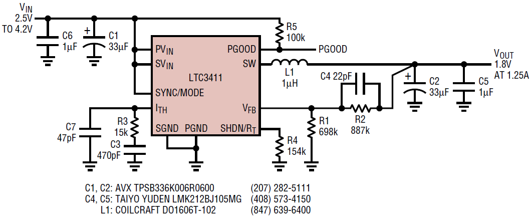
Figure 8a. Tiny 1.8V/1.25A step-down converter uses low profile components
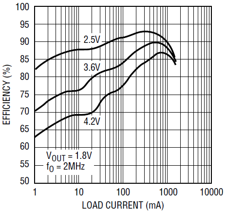
Figure 8b. Efficiency for the circuit in Figure 8a
The downside to running at a higher frequency is that efficiency suffers a little due to higher switching losses. The efficiency for this particular circuit peaks at 93% with VIN = 2.5V.
Conclusion
The LTC3411 is a monolithic, step-down regulator that switches at high frequencies, lowering component costs and board real estate requirements of DC/DC converters. Although the LTC3411 is designed for basic buck applications, its architecture is versatile enough to produce an efficient single inductor, positive buck-boost converter, due in part to its power saving Burst Mode operation and the OPTI-LOOP compensation feature.


