LTC1710: Two 0.4Ω Switches with SMBus Control Fit into Tiny MSOP-8 Package
LTC1710: Two 0.4Ω Switches with SMBus Control Fit into Tiny MSOP-8 Package
著者
Peter Guan
1998年05月01日
Introduction
The LTC1710 SMBus dual switch is a complete solution for supplying power to portable-equipment peripherals without the need for external switches. Two internal high-side N-channel switches, each capable of delivering 300mA at an RDS(ON) of 0.4Ω, are available in the tiny MSOP-8 package. With a low standby current of 14µA, the LTC1710 operates on an input voltage of 2.7V to 5.5V while maintaining the SMBus-specified 0.6V VIL and 1.4V VIH input thresholds
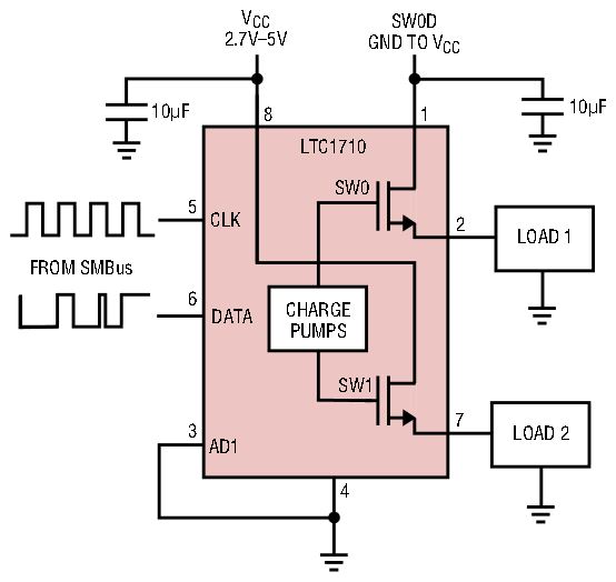
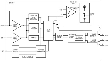
Figure 1 shows a typical application of the LTC1710 switching two different SMBus peripherals. Figure 2 shows a block diagram of the LTC1710 architecture, which can be broken down into four basic building blocks: the two N-channel power MOSFETs, the regulated charge-pump driver, the power-on reset and undervoltage-lockout units and the SMBus interface components.

Figure 1. Typical application: the LTC1710 switches two SMBus peripherals.

Figure 2. LTC1710 block diagram.
Two 0.4Ω Switches in MSOP-8
To fully enhance the power switches, the LTC1710 uses a charge-pump tripler to boost and regulate the gate drive of each switch. Running at about 300kHz, each charge pump is programmed to supply a ramped voltage to the gate of the switch, so that it turns on slowly and smoothly, avoiding large current spikes into the load. Since the charge pumps drive only the gates of the switches, only a small amount of current is needed; hence, the charge-pump caps are integrated on the IC.
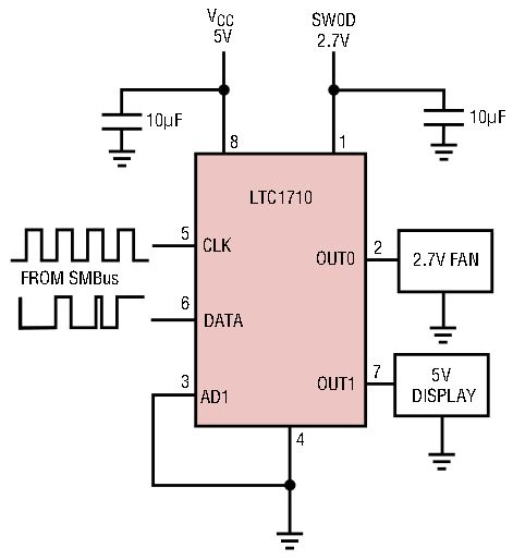
The drains of the two N-channel switches are independent of each other. Switch 1’s drain is connected to VCC, but the potential of switch 0’s drain can be anywhere between VCC and GND. As a result, SMBus peripherals requiring different input voltages can be simultaneously switched by the LTC1710 (Figure 3).

Figure 3. The LTC1710 switches two SMBus peripherals with different input voltages.
Though unlikely in normal operating conditions, if the internal switches become extremely hot as a result of sourcing too much output current, an internal thermal shutdown circuit becomes active at around 120°C and turns off the switch outputs temporarily until the temperature drops by about 15°C.
Power-On Reset and Undervoltage Lockout
To ensure that the LTC1710 starts up with both switches off, an internal power-on reset (POR) signal inhibits operation until about 300µs after VCC crosses the undervoltage lockout threshold (UVLO, typically 2V). The circuit also includes some hysteresis and delay to avoid nuisance resets. Once operation begins, VCC must drop below the UVLO threshold for at least 100µs to trigger another POR sequence.
Three-State Programmable Address Pin
To identify itself on the SMBus, the LTC1710 has a three-state programmable address pin (AD1) that can be tied directly to VCC, to GND or to VCC/2 with the help of two 1M resistors. To conserve standby current, it’s preferable to tie the address pin to either VCC or GND. The third state of VCC/2 should be used only when more than two addresses are needed on the bus. The three available addresses are 1011000 (AD1 = GND), 1011010 (AD1 = VCC) and 1011001 (AD1 = VCC/2). Notice that the five MSBs of the LTC1710 addresses are hardwired to 10110XX, which, according to the SMBus specifications, places the LTC1710 directly in the reserved address range for power-plane switching.
SMBus Operation
The SMBus is a serial bus interface that uses only two bus lines, DATA and CLK, to control low power peripheral devices in portable equipment. The LTC1710 is a slave-only device that uses the Send Byte protocol of the SMBus for communication. The master of the bus initiates communication to its slave devices with the Start signal, which is the switching of the DATA line from high to low while CLK is high. Upon detecting this Start signal, all slave devices on the bus, including the LTC1710, wake up and get ready to shift in the data that will follow. Beginning on the next rising CLK edge, the master sends out the first byte. The first seven bits of this byte consist of the address of the slave with which the master wishes to communicate. The last bit indicates whether the following command will be a read (logic one) or write (logic zero). Since the LTC1710 is a slave device that can only be written to by a master, it will ignore the read command, even if the address matches. If the first byte does match, then the LTC1710 will acknowledge proper reception to the master by pulling the DATA line low during the next CLK cycle. The master then sends the command byte with its two LSBs as the controlling signal for the switch outputs. A logic one turns on the internal charge pump to drive up the gate voltage and the output. A logic zero shuts down the charge pump and discharges the output to zero. After reception of the second byte, the LTC1710 again acknowledges the master by pulling DATA low for the next CLK cycle. At this point, valid data is shifted into the output latch of the LTC1710. However, the output switch won’t be enabled until the Stop signal (DATA going from low to high while CLK is high) is detected. With this double buffering feature of the output latch in the LTC1710, the Stop signal not only indicates an end to the Send Byte protocol, but can also be used to synchronize the output executions of several differently addressed SMBus peripherals whose valid data were also loaded into their respective output latches at different times without a Stop signal being sent. However, if a Start or Stop signal is detected in the middle of a byte transmission, the LTC1710 will regard it as an error and reject all previous data. An example of a Send Byte protocol is provided in Figure 4.

Figure 4. SMBus Send Byte protocol.
Conclusion
With two built-in 0.4Ω power switches in an MSOP-8 or SO-8 package and a low standby current (typically 14µA), the LTC1710 is an ideal and complete solution for delivering up to 300mA of current to SMBus peripherals in today’s complex portable equipment.


