Level Shift Allows CFA Video Amplifier to Swing to Ground on a Single Supply
Level Shift Allows CFA Video Amplifier to Swing to Ground on a Single Supply
著者
Frank Cox
1998年11月01日
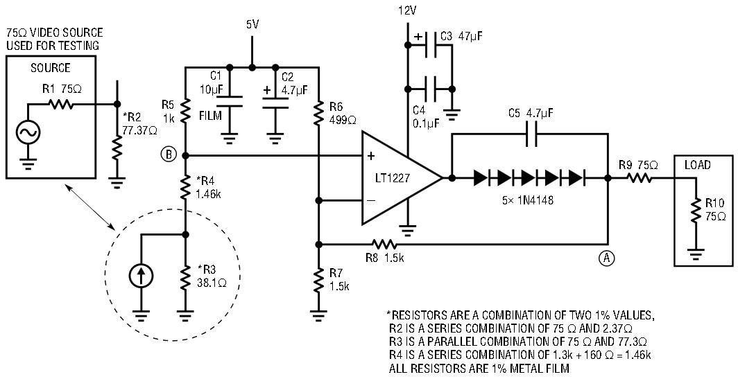
A current feedback (CFA) video amplifier can be made to run off a single supply and still amplify ground-referenced video with the addition of a simple and inexpensive level shifter. The circuit in Figure 1 is an amplifier and cable driver for a current output video DAC. The video can be composite or component but it must have sync. The single positive supply is 12V but could be as low as 6V for the LT1227.

Figure 1. Amplifier and cable driver for current-output video DAC.
The output of the LT1227 CFA used here can swing to within 2.5V of the negative supply with a 150Ω load over the commercial temperature range of 0°C to 70°C. Five diodes in the feedback loop are used, in conjunction with C5, to level shift the output to ground. The video from the output of the LT1227 charges C5 and the voltage across it allows the output to swing to ground or even slightly negative. However, the level of this negative swing will depend on the video signal and so will be unpredictable. When the scene is black, there must be sync on the video for C5 to remain charged. A zero-level component video signal with no sync will not work with this circuit. The CFA output will try to go to zero, or as low as it can, and the diodes will turn off. The load will be disconnected from the CFA output and connected through the feedback resistor to the network of R6 and R7. This causes about 150mVDC to appear at the output, instead of the 0V that should be there.
The ground-referenced video signal at the input needs to be level shifted into the input common mode range of the LT1227 (3V above negative supply). R4 and R5 shift the input signal to 3V. In the process, the input video is attenuated by a factor of 2.5. For correct gain, no offset and with a zero source impedance, R4 would be 1.5k. To compensate for the presence of R3, R4 is made 1.5k minus R3, or 1.46k. The trade off is a gain error of about 1.5%. If R4 is left 1.5k, the gain is correct, but there is an offset error of 75mV. R6, R7 and R8 set the gain and the output offset of the amplifier. A noninverting gain of five is taken to compensate for the attenuation in the input level shifter and the cable termination.
The voltage offset on the output of this circuit is a rather sensitive function of the value of the input resistors. For instance, an error of 1% in the value of R6 will cause an offset of 30mV (1% of 3V) on the output. This is in addition to the offset error introduced by the op amp. Precision resistor networks are available (BI technologies, 714-447-2345) with matching specifications of 0.1% or better. These could be used for the level shifting resistors, although this would make adjustments like the one made to R4 difficult.
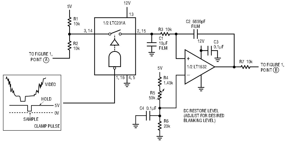
Fortunately, there is always synchronization information associated with video. A simple circuit can be used to DC restore voltage offsets produced by resistor mismatch, op amp offset or DC errors in the input video. Figure 2 shows the additional circuitry needed to perform this function. The LTC201A analog switch and C1 store the offset error during blanking. The clamp pulse should be 3µs or wider and should occur during blanking. It can conveniently be made by delaying the sync pulse with one shots. If the sync tip is clamped, the clamp pulse must start after and end before the sync pulse or offset errors will be introduced. The integrator made with the LT1632 adjusts the voltage at point B (see Figure 1) to correct the offset.

Figure 2. DC restore subcircuit.


