Industry’s First 0.8µVRMS Noise LDO Has 79dB Power Supply Rejection Ratio at 1MHz
Industry’s First 0.8µVRMS Noise LDO Has 79dB Power Supply Rejection Ratio at 1MHz
著者
Amit Patel
2015年04月01日
When it comes to powering noise-sensitive analog/RF applications, low dropout (LDO) linear regulators are generally preferred over their switching counterparts. Low noise LDOs power a wide range of analog/RF designs, including frequency synthesizers (PLLs/VCOs), RF mixers and modulators, high speed and high resolution data converters (ADCs and DACs) and precision sensors. Nevertheless, these applications have reached capabilities and sensitivities that are testing the limits of conventional low noise LDOs.
For instance, in many high end VCOs, power supply noise directly affects the VCO output phase noise (jitter). Moreover, to meet overall system efficiency requirements, the LDO usually post-regulates the output of a relatively noisy switching converter, so the high frequency power supply rejection ratio (PSRR) performance of the LDO becomes paramount. With its ultralow output noise and ultrahigh PSRR performance, the LT3042 can directly power some of most noise-sensitive applications while post-regulating the output of a switching converter, without requiring bulky filtering. Table 1 compares the LT3042’s noise performance with conventional low noise regulators.
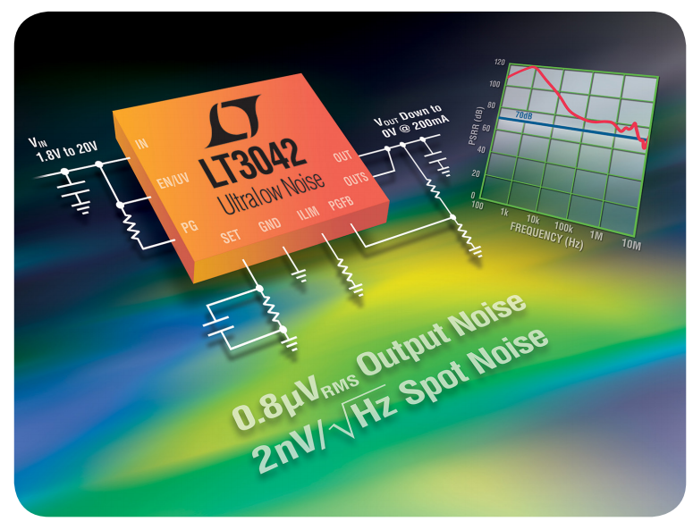
The LT3042 bring noise-free power to high performance electronics
| Parameter | LT1763 | LT3062 | LT3082 | LT3042 |
| RMS Noise (10Hz to 100kHz) | 20µVRMS | 30µVRMS | 33µVRMS | 0.8µVRMS |
| Spot Noise (10kHz) | 35nV/√Hz | 80nV/√Hz | 100nV/√Hz | 2nV/√Hz |
| PSRR at 1MHz | 22dB | 55dB | 45dB | 79dB |
| Minimum PSRR (DC to 1MHz) | 22dB | 30dB | 40dB | 77dB |
| Directly Parallelable | ✓ | ✓ | ||
| Programmable Current Limit | ✓ | |||
| Programmable Power Good | ✓ | |||
| Fast Start-up Capability | ✓ | |||
| Rail-to-Rail Output Range | ✓ | |||
| Quiescent Current | 30µA | 45µA | 300µA | 2mA |
Performance, Robustness & Simplicity
The LT3042 is a high performance low dropout linear regulator featuring Linear Technology’s ultralow noise and ultrahigh PSRR architecture for powering noise-sensitive applications. Even with its high performance, the LT3042 maintains simplicity and robustness. Figure 1 is a typical application and Figure 2 shows a complete demonstration circuit. The LT3042’s tiny 3mm × 3mm DFN package and minimal component requirements keep overall solution size small.
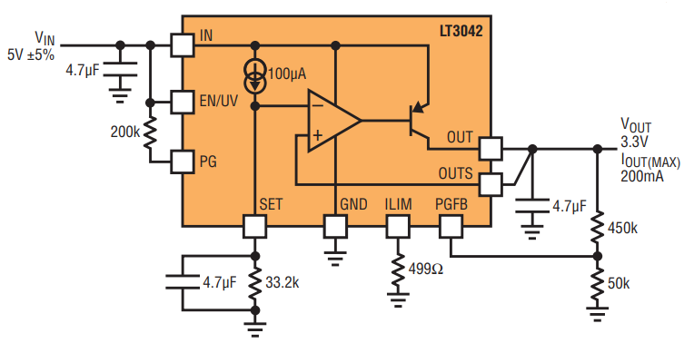
Figure 1. Typical LT3042 application.
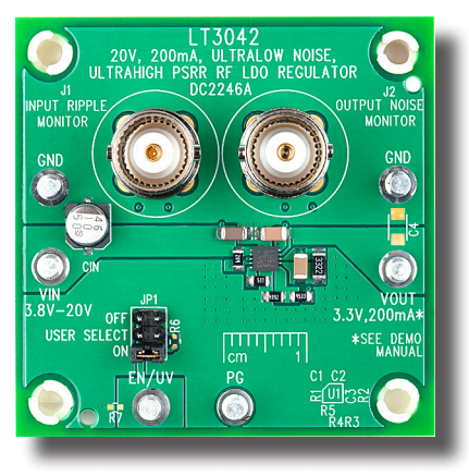
Figure 2. LT3042 demonstration circuit.
Designed as a precision current reference followed by a high performance voltage buffer, the LT3042 is easily paralleled to increase output current, spread heat on the PCB and further reduce noise—output noise decreases by the square-root of the number of devices in parallel. Its current-reference based architecture offers wide output voltage range (0V to 15V) while maintaining unity-gain operation, thereby providing virtually constant output noise, PSRR, bandwidth and load regulation, independent of the programmed output voltage.
In addition to offering ultralow noise and ultrahigh PSRR performance, the LT3042 includes features desired in modern systems, such as programmable current limit, programmable power good threshold and fast start-up capability. Furthermore, the LT3042 incorporates protection features for battery-powered systems. Its reverse input protection circuitry tolerates negative voltages at the input without damaging the IC or developing negative voltages at the output—essentially acting as if an ideal diode is connected in series with the input. In battery backup systems where the output can be held higher than the input, the LT3042’s reverse output-to-input protection circuitry prevents reverse current flow to the input supply. The LT3042 includes internal foldback current limit, as well as thermal limit with hysteresis for safe-operating-area protection.
Ultralow Output Noise
With its 0.8µVRMS output noise* in 10Hz to 100kHz bandwidth, the LT3042 is the industry’s first sub-1µVRMS noise regulator. Figure 3 compares the LT3042’s integrated output noise from 10Hz to 100kHz to that of the LT1763, Linear’s lowest noise regulator for over a decade. The LT3042’s ultralow noise performance opens up applications that were previously not possible, or otherwise required expensive and bulky filtering components.
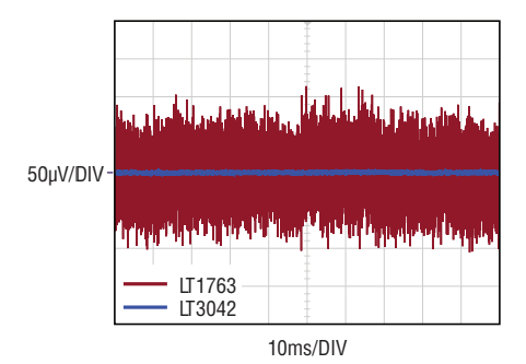
Figure 3. Output noise: 10Hz to 100kHz.
The SET pin capacitor (CSET) bypasses the reference current noise, the base current noise (of the error amplifier’s input stage) and the SET pin resistor’s (RSET) inherent thermal noise. As shown in Figure 4, low frequency noise performance is significantly improved with increasing CSET. With a 22µF CSET, the output noise is under 20nV/√Hz at 10Hz. Note that capacitors can also produce 1/f noise, particularly electrolytic capacitors. To minimize 1/f noise, use ceramic, tantalum or film capacitors on the SET pin.
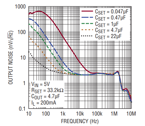
Figure 4. Noise spectral density.
Actively driving the SET pin with either a battery or a lower noise voltage reference reduces noise below 10Hz. Doing so essentially eliminates the reference current noise at lower frequencies, leaving only the extremely low error amplifier noise. This ability to drive the SET pin is another advantage of the current-reference architecture. The integrated RMS noise also improves as the SET pin capacitance increases, dropping below 1µVRMS with just 2.2µF CSET, as shown in Figure 5.
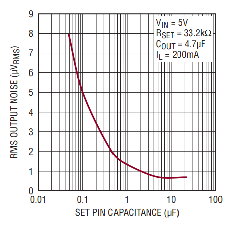
Figure 5. Integrated RMS output noise (10Hz to 100kHz).
Increasing SET pin bypass capacitance for lower output noise generally leads to increased start-up time. But the LT3042’s fast start-up circuitry alleviates this trade-off. The fast start-up circuitry is easily configured using two resistors; Figure 6 shows the significant improvement in start-up time.
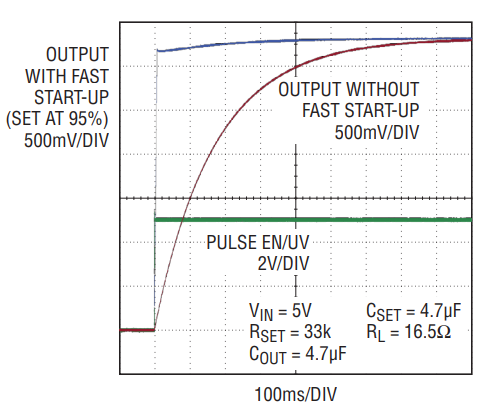
Figure 6. Fast start-up capability.
Ultrahigh PSRR Performance
LT3042’s high PSRR* is important when powering noise-sensitive applications. Figure 7 shows the LT3042’s incredible low and high frequency PSRR performance—approaching almost 120dB at 120Hz, 79dB at 1MHz, and better than 70dB all the way to 3MHz. PSRR performance is even better with decreasing load currents, as shown in Figure 8.
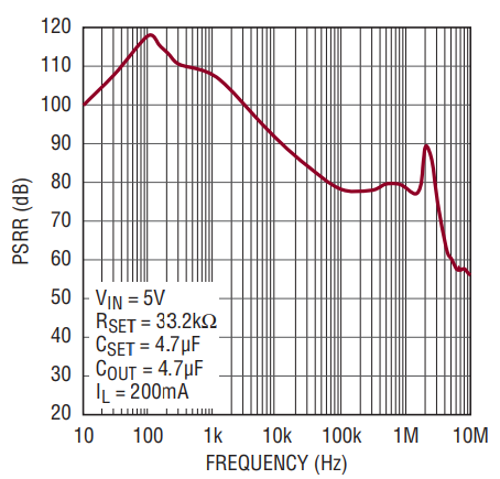
Figure 7. PSRR performance.
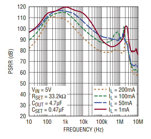
Figure 8. PSRR for various load currents.
Unlike conventional LDOs whose PSRR performance deteriorates into the 10s of dB as you approach dropout, the LT3042 maintains high PSRR at even low input-to-output differentials. As Figure 9 illustrates, LT3042 maintains 70dB PSRR up to 2MHz with only 1V input-to-output differential and almost 60dB PSRR up to 2MHz at a mere 600mV input-to-output differential. This capability allows the LT3042 to post-regulate switching converters at low input-to-output differentials—for high efficiency—while its PSRR performance satisfies the requirements of noise-sensitive applications.
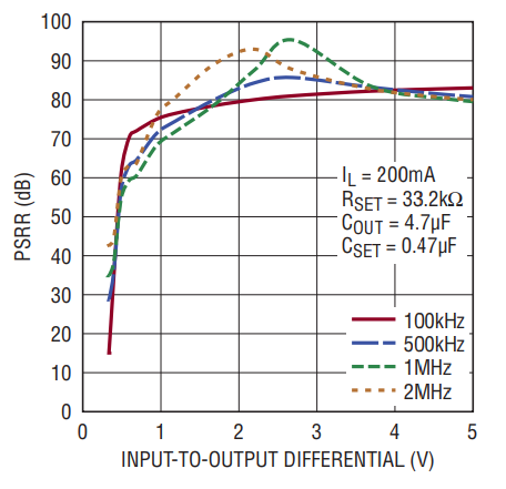
Figure 9. PSRR vs input-to-output differential.
Post-Regulating A Switcher
In applications where the LT3042 is post-regulating the output of a switching converter to achieve ultrahigh PSRR at high frequencies, care must be taken with the electromagnetic coupling from the switching converter to the output of the LT3042. In particular, while the “hotloop” of the switching converter should be as small as possible, the “warm-loop” (with AC currents flowing at the switching frequency) formed by the switcher IC, output inductor, and output capacitor (for a buck converter) should also be minimized, and it should either be shielded or placed a couple of inches away from ultralow noise devices like the LT3042 and its load. While the LT3042’s orientation with respect to the “warm-loop” can be optimized for minimum magnetic coupling, it can be challenging in practice to achieve 80dB of rejection simply with optimized orientation—multiple iterations of the PC board may be required.
Consider Figure 10, where the LT3042 is post-regulating the LT8614 Silent Switcher® regulator running at 500kHz with an EMI filter at switching regulator input. With the LT3042 located just one to two inches from the switching converter and its external components, almost 80dB rejection at 500kHz is achieved without any shielding.
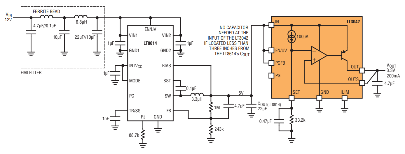
Figure 10. The LT3042 post-regulating LT8614 Silent Switcher regulator.
To achieve this performance, however, as Figure 11a highlights, no additional capacitor—other than the 22µF at switcher’s output—is placed at the input of the LT3042. However, as shown in Figure 11b, even placing a small 4.7µF capacitor directly at the input of the LT3042 results in over 10× degradation in PSRR.
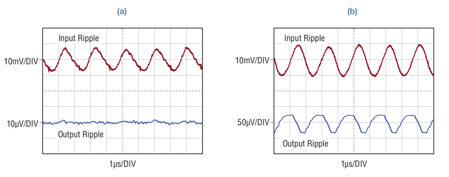
Figure 11. The LT3042 post-regulating the LT8614 Silent Switcher (a) without any capacitor at the LT3042 input, (b) with a 4.7µF capacitor at LT3042 input.
This is peculiarly counter-intuitive—adding input capacitance generally reduces output ripple—but at 80dB rejection, the magnetic coupling, which is usually insignificant, resulting from moderately high frequency (500kHz) switching currents flowing though this 4.7µF capacitor, significantly degrades output ripple. While changing the orientation of the 4.7µF input capacitor and the traces connecting the switcher’s output to this capacitor help minimize magnetic coupling, it remains rather difficult to achieve nearly 80dB of rejection at these frequencies, not to mention the multiple PC board iterations it may require.
The relatively high input impedance of the LT3042 prevents high frequency AC currents from flowing to its input terminal. Given that the LT3042 is stable without an input capacitor if located within three inches of the pre-regulating switching power supply’s output capacitor, to achieve best PSRR performance, we recommend not placing a capacitor at the LT3042’s input, or minimizing it.
A couple of inches of trace inductance connecting the LT8614 to the LT3042 input significantly attenuates the very high frequency power switch transition spikes. Some spikes still propagate to the output due to magnetic coupling from the LT8614’s “hot-loop.” Optimizing the LT3042 board orientation reduces the remaining spikes. Due to instrumentation bandwidth limitation, these very high frequency spikes are not shown in Figure 11’s output ripple.
For perspective, trying to achieve 80dB rejection at 500kHz without using the ultrahigh PSRR LT3042 LDO is a tall order. Alternatives don’t measure up. For instance, an LC filter would require nearly 40µH of inductance and 40µF of capacitance to achieve 80dB rejection at 500kHz, adding large, expensive components. Costs and board real estate aside, the LC can resonate if not properly damped, adding complexity. Using an RC filter is untenable, requiring impractical resistance to achieve 80dB rejection. Similarly, using conventional LDOs require cascading at least two of them to achieve 80dB rejection at 500kHz, which requires additional components and cost, and degrades the dropout voltage.
Additionally, to achieve 80dB rejection, these alternatives also require attention to magnetic field couplings. In particular, high frequency AC currents must be minimized.
Owing to its ultrahigh PSRR over a wide frequency range, the LT3042 allows lower frequency operation of the upstream switching converter—for improved efficiency and EMI—without requiring any increase in filter component size for powering noise-sensitive applications.
Conclusion
The LT3042’s breakthrough noise and PSRR performance, coupled with its robustness and ease-of-use, make it ideal for powering noise-sensitive applications. With its current-reference based architecture, noise and PSRR performance remain independent of the output voltage. Additionally, multiple LT3042s can be directly paralleled to further reduce output noise, increase output current and spread heat on the PCB.
Notes
* Proper measurement of noise and PSRR at these levels requires extreme care and special instrumentation. These measurement processes will be comprehensively treated in a forthcoming Linear Application Note.
著者について
Amit Patel is a senior design manager at Analog Devices Inc. (ADI) responsible for all new LDO product development. He has been with Linear Technology/ADI for 11 years, starting as a design engineer in the Power Products g...


