How to Excite Off Board Sensors and Loads
In distributed systems, analog signals are transmitted remotely to or from sensors or loads. In this type of system the signal travels long distances and the noise robustness becomes a major concern. The noise couples into the signal corrupting the data and generating an undesirable effect. The system needs to be correctly protected, and understanding the amount and nature of the expected noise will define the necessary protection that needs to be implemented to cancel or at least minimize the level of environmental disturbances.
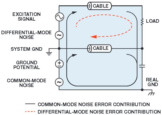
There are two different sources of noise or interference—depending on how they get coupled into the main signal, common-mode and differential-mode noise, as shown in Figure 1.

Figure 1. Noise sources.
The less harmful of these is the common-mode noise, which is added to both system GND and excitation signal simultaneously, mainly due to a dipole antenna effect between cables and real GND. It does not degrade the signal as the noise is coupled simultaneously in both channels with similar magnitude. The problem is that common-mode noise generates a signal offset that lifts real GND, which has two undesirable effects. Firstly, it could saturate the load if it is indirectly referenced to real GND, for example, when the sensor is protected by a metal box. Secondly, it could generate an electric arc, damaging the sensor. Common-mode noise is especially problematic when exciting a Wheatstone bridge as the output signal needs to be processed by the controller, typically using an instrumentation amplifier, which offers a finite CMRR and consequently noise could be amplified.
Common-mode noise can be minimized by filtering the input signal using low-pass filters (for example, RC filter) or by using common-mode choke coils. An important point is that common-mode noise asymmetrically attenuated generates differential mode noise. A practical example of asymmetrical attenuation is a low-pass filter; the cut-off frequency is implemented by a resistor and capacitor but due to component tolerances the cut-off frequencies are not the same in both lines.
The second, and most problematic is the differential-mode noise, which is coupled between excitation and system GND. This noise is coupled to the signal due to current loops between system GND and the signal cables that act as an antenna. In some applications, like chemical analysis, the sensor is sometimes placed in a chamber separated from the controller for security reasons. This setup creates current loops of tens or hundreds of meters and, consequently, any magnetic flux can induce current noise on the signal, corrupting the data. To minimize the differential-mode noise contribution, it is recommended ferrites are used to filter high frequency radiated signals, star connections between controller and sensors, and shielding cables.
In both cases, if the noise is large enough, it could even damage the equipment due to electrical overstress. This is particularly true when the load is a motor or a fluorescent lamp, which provides a strong source of EMC/EMI; firstly due to the physical electromagnetic components, and secondly due to the nature of the signal generated. It is always good practice to use EMC/EMI suppressors like ESD protection to guarantee some level of system robustness.
The main consequence of implementing some of the methods described previously is the capacitance associated with the components. Even cables consist of parasitic capacitance and, consequently, cannot be omitted. The parasitic capacitance is proportional to the length, type, and category of the cable, as shown in Table 1.
| Type | Category | Description | Capacitance (pF/m) |
| Twisted | 5 | Unshielded cable, unshielded twisted pair | 52 |
| 6a | Foil shielded cable, unshielded twisted pair | 5 | |
| 7 | Foil shielded cable, foil shielded twisted pair | 42 | |
| Coaxial | RG-59/U RG-214/U |
Single shielded, doubled shielded | 67 100 |
Integrated buffer voltage DACs, like the AD5683R or AD5686R, are designed to provide high slew rates and bandwidth with reduced power consumption, which is becoming a major concern for a number of reasons—such as reduced board temperature, an increase in the number of components per board (without increasing power), and improved power efficiency. As a result, the internal amplifier impedance, ZO (open-loop impedance), is big (do not confuse with ZOUT— closed-loop impedance), limiting the maximum load capacitance.
If the capacitance connected to the op amp output exceeds the maximum allowable value, the op amp stability is compromised and, consequently, the amplifier could ring and oscillate.
There are few methods to minimize the op amp instability using buffered voltage DACs:
- RSHUNT method
- External load network compensation, snubber method
The RSHUNT method requires minimum external components, the idea behind this method is relatively simple; the op amp is isolated from the load by placing a discrete resistance in between.
The RSHUNT adds a zero in the transfer function of the feedback network, which makes the close loop stable at high frequencies. The zero should be chosen at least one decade below the GBP (gain bandwidth product). The problem in this case is that the DAC specifications do not include this number as it is irrelevant because the internal op amp is used as a buffer.
In this case, rule of thumb recommends to select a value as low as possible to minimize the resistance performance contribution; 5 Ω to 50 Ω resistance is a common range. If this method is used, the load voltage drops, as physically this is implemented as a resistor voltage divider, impacting other specifications such as lower slew rate and settling time. Consequently, overall DACspecifications from the load or sensor side are degraded.
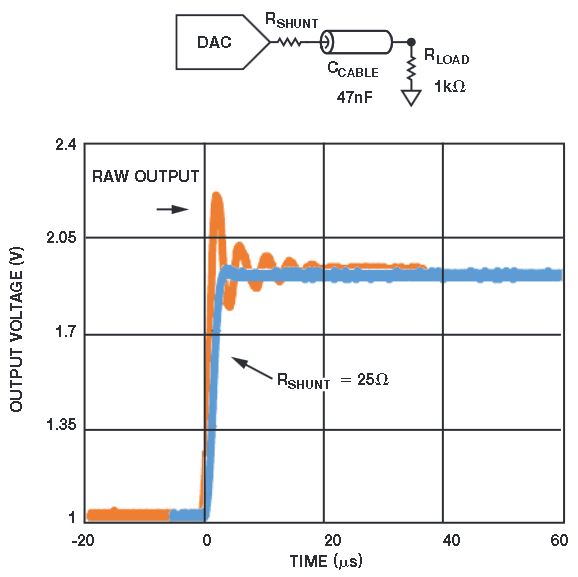
By increasing the RSHUNT value, the damping ratio (ζ) is increased, making it a suitable method for driving motors, but it is not recommended when the magnitude of the load is small and the voltage rails are low, like in a Wheatstone bridge excitation, as the drop in amplitude could be considerable. Reducing the voltage span, for instance, using 5 V rails in a 1 kΩ impedance, the drop is around 2.5% as shown in Figure 2.

Figure 2. RSHUNT method.
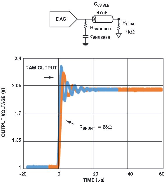
The snubber method (or RC shunt) does not reduce the load voltage span so it is preferred for low voltage applications. The idea behind this method is slightly different. The snubber network decreases the impedance of the load close to the oscillation frequency, making the real part of the load lower than the imaginary and consequently changing the phase.
The correct component value selection used needs to be determined empirically by analyzing the transient response of the DAC connected to the load.
Typically, calculations are based on the assumption that the buffer GBP is below 1 MHz. In this case, assuming a 47 nF parasitic cable capacitance,

The ideal resistance should be below 1 Ω, the lower the RSNUBBER value, the lower the overshoot but from a practical point of view, let’s select RSNUBBER = 10 Ω.
The snubber pole needs to be ¹⁄³ above oscillation frequency,


Figure 3. Snubber method.
Snubber and shunt methods are extremely useful to compensating or isolating a capacitive load, making the DAC stable when the load or sensor needs to be excited remotely.
The above examples are based on the AD5683RDAC, which due to the ultra-small package and overall performance, 2 LSB INL @ 16 bits, 35 mA drive capability, integrated reference, and robustness, 4 kV ESD, makes it an ideal DAC for exciting loads or off board sensors.


