Hot Swap Controller Monitors and Reports Power Supply Status
Introduction
High availability systems are designed to achieve an ideal of zero down time. To approach this goal, the system needs to be able to operate during routine maintenance and upgrades, which often involves cards being inserted and removed from a live backplane. These systems must also be designed for failsafe operation by isolating faulty boards before they cause backplane disturbances.
Hot swapping requires a power switch to initially isolate the board, and a controller to turn on the switch slowly to minimize backplane disturbances. Since the Hot Swap controller monitors card voltage and current, it is an obvious place to integrate higher level monitoring with a data converter. This provides detailed information about the health of the power path and the power consumption of downstream circuits. Such information can be used to monitor performance over time and identify boards that are drifting towards failure or marginal performance.
The LTC4215 combines a robust Hot Swap circuit with an I2C interface and data converter to allow power monitoring as well as hot-plug functionality and fault isolation (see Table 1). In a typical application the LTC4215 uses an external N-channel pass transistor to isolate the hot swapped board from the backplane when it is first inserted (Figure 1). After a debounce time the controller can begin to apply power to the board or wait for a turn-on command from a host processor. Power is ramped gradually to minimize any backplane disturbance. After the power-up process is complete, the LTC4215 continues to monitor for faults in the power path.
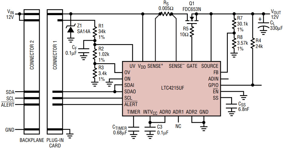
Figure 1. In a typical application the LTC4215 uses an external N-channel pass transistor to isolate the hot swapped board from the backplane when it is first inserted. After a debounce time the controller can begin to apply power to the board or wait for a turn-on command from a host processor. Power is ramped gradually to minimize any backplane disturbance. After the power-up process is complete, the LTC4215 continues to monitor for faults in the power path.
| Feature | Benefits |
| Wide Input Voltage Range: Operates from inputs of 2.9V to 15V, with 24V absolute maximum | ❏ Suitable for 3.3V, 5V and 12V systems ❏ Simplifies design because part functions on a semi-regulated supply ❏ Large overvoltage transient range eases design tolerances for transient protection |
| 8-bit ADC: ADC monitors current, output voltage and external pin voltage and measures off-state current in the FET to determine FET failures | ❏ Increases reliability ❏ Board power information provides an early warning of board failure ❏ Verify board is staying within its allotted power ❏ Allows integrity check of redundant supply paths ❏ Allows active power management to safely maximize power utilization within the chassis cooling constraints |
| I2C/SMBus: Communicates as a read-write slave device using a 2-wire serial interface | ❏ Improves integration with the host system. Interface allows the host to configure the part, determine which faults are present or have occurred, and read back ADC measurements |
| Fast Short Circuit Response: Fast (<1µs) current limit response to shorts | ❏ Protects connector from overcurrent ❏ Limits the disturbance to the input supply from a short circuit |
| Alerts Host after Faults: When configured (using I2C), faults activate an active pull-down on the ALERT pin |
❏ Interrupting the host for immediate fault servicing limits system damage ❏ Reduces the bus traffic for polling |
The LTC4215 provides the means for quantitatively measuring the board current and voltages with an onboard ADC and multiplexer. It reports this information using the I2C serial communication bus when polled by a host processor. The device interrupts the host for specific fault conditions, if configured to do so.
The LTC4215 works in applications from 12V (with transients to 24V) down to 3.3V where the operating input voltage could drop to 2.9V. Functionally, the LTC4215 is very similar to the LTC4260 (Linear Technology, Nov. 2004) operating in a lower voltage range. Table 2 compares the major features of the LTC4215 and LTC4260. Special attention should be paid to the power-up sequence because of the added soft start pin and some changes in the function of the TIMER pin relative to the LTC4260. Since both parts can be used for 12V systems, Table 2 may be used to select the part with optimal set of features for a specific 12V application.
| Feature | LTC4215 | LTC4260 |
| VDD Abs Max | 24V | 100V |
| VDD Min | 2.9V | 8.5V |
| Recommend TransZorb for 12V | Yes | No |
| Current Limit/Circuit Breaker | 25mV | 50mV |
| Circuit Breaker Precision | 10% | 10% |
| Current Limit Precision (FB = 0) | 35% | 25% |
| Current Limit vs Circuit Breaker VTH | 75mV, 25mV | Both 50mV |
| Current Limit Foldback | Only during startup | Always |
| Gate RC Network | Optional | Required |
| Soft Start | Yes, Required | No |
| Timer Pin | Optional | Required |
| OC Timer | 20µs | External/Adjustable |
| ∆VGATE at 12V (0µA) | 6V | 8.5V |
| Built In Overvoltage Threshold | 15.6V | None |
| ADC Source LSB | 60mV | 400mV |
| ADC VSENSE LSB | 151µV | 300µV |
| ADC ADIN LSB | 4.85mV | 10mV |
| Internally Generated VCC | 3.1V | 5.5V |
| Package | 4mm × 5mm QFN | 5mm × 5mm QFN |
An N-channel pass transistor, Q1, controls the application of power to the board as in Figure 1. A series sense resistor, RS, allows the LTC4215 to measure the current in the powerpath. Resistor R5 suppresses self oscillations in Q1. Resistors R1–R3 select the undervoltage (UV) and overvoltage (OV) thresholds. Capacitor CF allows these thresholds to be filtered as needed. R7 and R8 select the powergood threshold and set the foldback current limit level. Capacitor CSS sets a maximum slew rate to control the inrush current and CTIMER is used to set the startup time. C3 is used to bypass the internal core voltage.
Typically, the pins on the connector are staggered so that bulk power is applied first with the longest pins, followed by communication lines on medium length pins, and last, Hot Swap control lines such as the supply for the UV, OV, or EN pins. The UV, OV and EN pins must be in the correct state for a programmable debounce period of 100ms before Q1 is allowed to turn on. At this point the ON pin turns the part on immediately if it is high, or holds the part off if it is low. When the ON pin is held low, Q1 is turned on through the I2C bus by writing to the ON bit in the control register.
Measure Real-Time Board Power with Integrated ADC
Monitoring the supply voltage and current in real-time is a useful way of tracking the health of the power path. New data can be compared with historical data for the same card to detect changes in power consumption that could indicate that the card is behaving abnormally. An abnormal card can be shut down and flagged for service, perhaps before a more severe fault or system malfunction occurs. The LTC4215 includes an 8-bit data converter that continuously monitors three voltages: the ADIN pin, the SOURCE pin and the current sense voltage between the SENSE+ (VDD) and SENSE– pins. The ADIN pin is an uncommitted ADC input which allows the user to monitor any available voltage.
The ADIN pin is monitored with a 1.235V full scale. The ADIN pin is connected directly to a data converter input without any signal scaling. The SOURCE pin uses a 1:12.5 divider at the input which gives a 15.4V full scale. The SENSE voltage amplifier has a voltage gain of 32, which results in a 38.4mV full scale. The converter uses a sophisticated oversampling and offset cancellation method that preserves the full 8-bit dynamic range on the SENSE channel.
If the data converter reads more than 1mV on the VDD-SENSE channel while the external switch is turned off, the LTC4215 generates a FET-SHORT fault to indicate that the switch may be damaged. The presence of this condition is indicated in STATUS register bit C5 and logged to FAULT register bit D5. The LTC4215 takes no action in this condition other than logging the fault and generating an alert if configured to do so.
The results from each conversion are stored in three ADC registers (see Table 3) and updated 10 times a second. Setting the test mode control register bit halts the data converter so that the registers can be written to and read from for software testing.
| Register | Description |
| CONTROL | Register turns-on or turns-off the pass transistor and controls whether the part will auto-retry or latchoff after a fault. It also configures the behavior of the GPIO pin. |
| ALERT | Alert register enables which faults interrupt the host using the ALERT pin. At power-up the default is to not alert on faults. |
| STATUS | Status register provides pass transistor (on/off), EN (high/low) and GPIO (high/low) conditions. It also lists five fault present conditions. |
| FAULT | Fault register logs overcurrent, overvoltage, undervoltage, power-bad, FET short and EN changed state faults. |
| SENSE | ADC data for the VDD-SENSE voltage measurement. |
| SOURCE | ADC data for the SOURCE pin voltage measurement. |
| ADIN | ADC data for the ADIN pin voltage measurement. |
Versatile Inrush Current Control
Once the inputs to the LTC4215 reach the correct values for the part to turn the external switch on and an internal 100ms debounce timer has expired, the LTC4215 turns on. The startup time is determined by the capacitor on the TIMER pin, or 100ms if the TIMER pin is tied to VCC. During this time the circuit breaker is disabled to prevent an overcurrent fault from occurring, the power-good signal from the GPIO pin is also disabled to prevent turning on a load before the current limit has reached the full value via the Soft Start and Foldback pins. The inrush current slew rate (dI/dt) is limited via the SS pin. The inrush current is also folded back from 25mV to 10mV via the FB pin. An optional RC network on the external MOSFET gate can be used to set the inrush current below the foldback level by setting the maximum slope of the output voltage. The various inrush current profiles obtainable by these three methods are detailed in Figures 2 thru 6, which show a 12V system with a 25mΩ sense resistor, or 1A current limit, starting up into a 470µF capacitive load.
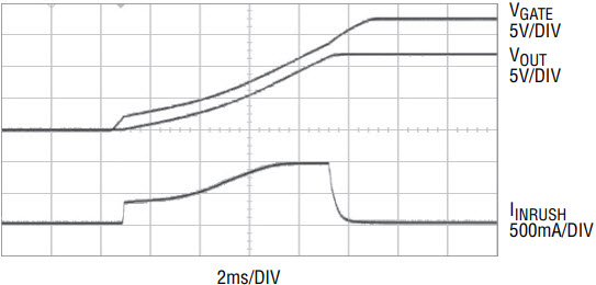
Figure 2. Inrush current is limited by foldback. This allows the fastest startup of the load, with the inrush only lasting 9ms with a peak current of 1A.
At the end of the startup period the current limit circuit is checked. If the current limit is still regulating the current, the LTC4215 determines that the output failed to come up and generates an overcurrent fault. If the current limit circuit is not active then the current limit threshold is moved to 75mV, the power-good signal to the GPIO pin is enabled and the 25mV circuit breaker is armed.
The SS pin sets the current slew rate limit at startup. It starts at ground, which corresponds to a negative voltage on the sense resistor and results in the MOSFET being turned off. A current into the soft-start capacitor produces a ramp that corresponds to increasing VDD-SENSE voltage. When the current limit circuit releases the gate (when the commanded VDD-SENSE voltage becomes positive) the current from the SS pin is stopped to wait for the GATE pin to rise and start to turn on the MOSFET. Once the current limit circuit begins to regulate the VDD-SENSE voltage, the current from the SS pin is resumed and the ramp continues until it reaches the foldback level. It is important that the SS pin stop the ramp while the GATE pin slews because the ramp would otherwise continue and result in an uncontrolled step in current once the MOSFET threshold is reached. An uncontrolled step may violate inrush specifications and cause supply glitches on the backplane.
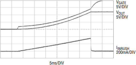
Figure 3. Inrush current is limited by a 1µF SS capacitor. This provides the fastest startup in a system with demanding inrush current slew rate requirements. Inrush dI/dt is reduced to 12mA/ms.
If the soft-start ramp reaches the foldback level, the foldback circuit stops the ramp, as shown in Figure 5. The ramp is allowed to continue as the voltage at the FB pin rises and increases the foldback current limit, still limited in slope and limited in magnitude by foldback as well.
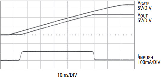
Figure 4. Inrush current is limited by a 0.1µF GATE capacitor. This minimizes the power in the switch, allowing the use of smaller components at the cost of speed. The inrush current is only 100mA, but startup takes 55ms.
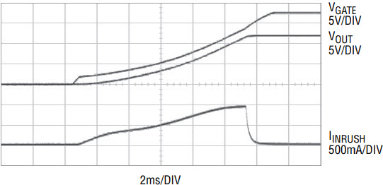
Figure 5. Inrush current is limited by a 68nF SS capacitor and FB. Soft start controls the inrush current slew rate while the current limit is modulated by foldback. This allows the fastest startup while also protecting the backplane from current surges.
If an RC network is placed on the GATE pin to manually set the inrush current to a value below the foldback level (Figure 4), the current limit circuit will leave regulation when it is unable to achieve the VDD-SENSE voltage commanded by the SS and FB pins. If the startup timer expires during this inrush an overcurrent fault is not generated because the current limit is not active. The power-good output for GPIO is allowed to relay the state of the FB pin, and the circuit breaker is armed. Either the output voltage finishes rising and a power good is asserted when the FB pin crosses it’s 1.235V threshold, or the current rises to the circuit breaker threshold and the part generates an overcurrent fault.
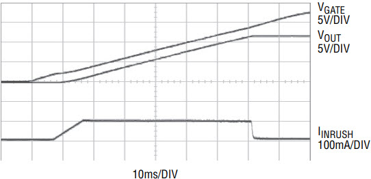
Figure 6. Inrush current with 1µF SS capacitor and 0.1µF GATE capacitor. Soft start limits the inrush current slew rate until the GATE capacitor limits the inrush current by limiting the dV/dt at the output. This minimizes the power in the switch while protecting the backplane from inrush current surges.
In the event there is an overcurrent condition after startup, the current limit circuit limits the VDD-SENSE voltage to 75mV while the circuit breaker waits for a 20µs timeout before producing an overcurrent fault. After any overcurrent fault, the part waits for a cool-down period of 50 times the startup time before allowing the part to restart by any means, including auto-retry, I2C, or cycling the EN, UV or ON pins.
Controlled Turn-Off
When the LTC4215 is turned off by a fault or I2C transaction, the GATE pin is pulled down with a 1mA current source. Once the GATE pin is below the SOURCE pin, a diode from SOURCE to GATE turns on and the voltage at the SOURCE pin is discharged by the same 1mA current.
If there is a short that causes the sense voltage to exceed 75mV, a 400mA pull-down from GATE to SOURCE removes the gate charge of the switch. Once the sense voltage falls to 75mV, the current limit regulates there for 20µs before turning the gate off with the 1mA current source.
If there is significant inductance between VDD (SENSE+) and bulk capacitance, across a connector for instance, it is possible that a short circuit at the output with a very fast rise time could cause the input voltage to collapse while the current through this inductance slews. In this case, after 2µs, the VDD undervoltage lockout circuit turns on and discharges the GATE pin with the 400mA pull-down to the SOURCE pin and quickly turns the switch off.
Save Power with Precise 25mV Circuit Breaker
For supplies with lower voltages and higher currents, a 50mV circuit breaker threshold may result in too much power dissipation in the sense resistor, or cut excessively into the input supply voltage tolerance of downstream circuits. To reduce this problem the LTC4215 has a precision circuit breaker at 25mV with a low 10% tolerance. This allows the use of smaller and less expensive sense resistors with lower power ratings.
In systems where the circuit breaker has only 20% accuracy the designer must be able to safely provide 40% more power than the card actually consumes to ensure that the slot doesn’t suffer from heat and supply limitations on the high side or produce a fault in normal operation on the low side. The precise 10% accuracy of the LTC4215 cuts this guard-band in half and safely allows the use of 20% more power than a slot with a 20% accurate circuit breaker.
Detect Insertion Events via the ENABLE
Pin
The EN pin can be used to sense the insertion of a board when the LTC4215 is used in backplane resident application. A short pin on the connector pulls EN to ground once the other, longer pins have already been connected. Once the EN pin crosses its falling 1.107V threshold the LTC4215 turns on the external switch after a 100ms debounce delay. Because a falling edge on the EN pin corresponds to the insertion of a new board, the LTC4215 clears the fault register (except for the EN Changed State bit) so that a previously recorded fault does not prevent the new board from starting up. Whenever the EN pin rises or falls, the EN Changed State bit in the FAULT register is set to indicate that a board has either been inserted or removed. A STATUS register bit contains the complement of the state of the EN pin to indicate if a board is present. When the board is unplugged, the short EN pin is the first to disconnect. The EN pin pulls up with an internal 10µA current source until the voltage reaches the rising 1.235V threshold, at which point the external switch is turned off with a 1mA current.
Conclusion
The LTC4215 is a smart power gateway for hot swappable circuits. It provides fault isolation, closely monitors the health of the power path and provides an unprecedented level of control over the inrush current profile. It logs faults, provides real-time status information, and can interrupt the host if necessary. Meanwhile an internal 8-bit ADC continuously monitors board current and voltages. These features make the LTC4215 an ideal power gateway for high availability systems.


