要約
Thin-film transistor-liquid crystal display (TFT-LCD) panels dominate the automotive display market as the size and resolution of in-car displays increase. These solutions require higher current with precision, flexibility, and small overall solution size and cost to meet increasingly stringent system requirements. The MAX25512 is a four-channel LED driver that integrates boost FET, current sense, and an I2C function. In this design solution, we review the key specifications of the MAX25512 and learn how to design it into the latest automotive display applications.
Introduction
Displays are ubiquitous in modern cars, from instrument clusters to center stack touchscreens (Figure 1), head-up displays, rear-seat entertainment, and more. It is estimated that there are up to 12 displays per vehicle in today’s automobiles. The vast automotive display market is dominated by TFT-LCD technologies while OLEDs may play a significant role in the future. For TFT-LCD panels, a majority is still white LED edge-lit displays, which need precise, constant current sink to drive these LEDs.
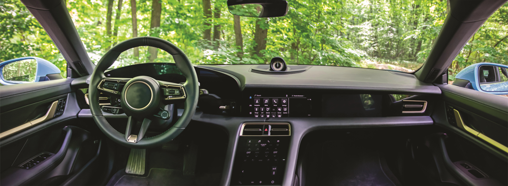
Typical TFT-LCD Display System
Figure 2 illustrates a simplified block diagram of a typical TFT-LCD automotive display. The display receives power through multiple rails while the video signal receives power through the gigabit multimedia serial link (GMSL). It converts serial LVDS data to a parallel interface in RGB format. A high-voltage buck converter provides the main 5V or 3.3V rail, which feeds the rest of the low-voltage circuits while the high-voltage LDO provides the always-on power to the MCU. The LED driver is usually directly connected to a car battery, which is needed to support lower battery voltage for start-stop systems as well as cold-crank conditions.
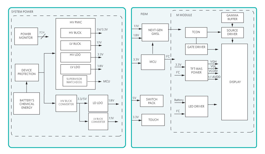
TFT-LCD LED Driver Needs
Automotive display sizes and resolutions are increasing, which means more current is needed. At the same time, engineers want greater integration to help save system solution size and cost. In addition, engineers want easier-to-use ICs to accommodate different projects and time-to-market pressure. The MAX25512 shown in Figure 3 is a 4-channel LED backlight driver IC with an integrated boost FET, current sense, and I2C interface to save solution size and cost. I2C interface/communication is needed for settings and diagnostics readout that make displays safer. This is especially important for instrument clusters, head-up displays, and side-mirror replacement displays. The MAX22512 IC can also support battery voltage down to 3V after startup, which is needed for cold-crank application without the need for additional pre-boost upfront. Using NMOS input current protection instead of PMOS can also save BOM cost. The backlight driver IC features I2C-controlled pulse-width-modulation (PWM) dimming and hybrid dimming. In either case, the minimum pulse width is 300ns, which helps achieve a dimming ratio of 16,666:1 with a PWM frequency at 200Hz. Hybrid dimming helps reduce EMI or improves the dimming ratio. Phase-shifted dimming of the strings and spread spectrum are also incorporated for lower EMI. Because diagnostics is critical for displays; this IC implements the following key features:
- Each string LED has open/short detection
- Boost output voltage and overvoltage detection
- Short to GND detection on each SINK
- Thermal warning and shutdown
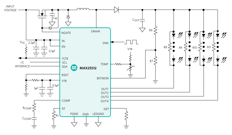
Design Example
Table 1 shows an automotive display application where the MAX25512 is used. This requires nine LEDs with 4 strings, each at 120mA, with an automatic 60° phase shift. The brightness control register is used for an LED dimming method through I2C communication. The boost controller operates at 2.2MHz boost switching frequency with spread spectrum enabled. Table 2 lists the components and their values.
| Design Parameter | Value |
| Input Voltage Range | 5.5V to 18V After startup, 3V/100ms |
| LED String Configuration | 4 strings 9 LEDs in series |
| Boost Output Voltage | 30V |
| LED String Current | 120mA |
| Switching Frequency | 2.1MHz |
| Brightness Control | I2C |
| Reference | Value | Description |
| CINPUT | 2 x 10µF | Capacitor, ceramic, 50V, X7R |
| L1 | 2.2µH | Inductor, ±20%, 8A |
| COUT | 3 x 10µF | Capacitor, ceramic, 50V, X7R |
Detailed Design Procedure
Selecting the appropriate component types and values ensures optimum device operation and allows the attainment of maximum efficiency and lowest noise operation. The following sections describe how to make critical design component selections and use I2C to control key parameters according to the application circuit shown in Figure 3.
Switching Frequency Selection
The internal oscillator frequency is programmable between 400kHz and 2.2MHz using a timing resistor connected from RT to GND. The value of the timing resistor (RRT) for the desired switching frequency (fSW) is calculated using the following equation:

where RRT and fSW are expressed in kΩ and Hz, respectively. RRT = 12.3kΩ sets a switching frequency of 2.1MHz.
Boost Converter Inductor Selection
To determine the inductance value, first select the ratio of inductor peak-to-peak ripple current to average current (LIR). The recommended value is 60% (LIR = 0.6).
The value of the inductor is determined as follows:
ILED = ISTRING x 4
where ISTRING is the LED string current in amperes.

where VD is the forward drop of the rectifier diode in volts (approximately 0.6V), VLED is the boost output voltage and VFET is the drain-to-source voltage of the internal MOSFET when it is on. It can be calculated by:

0.125Ω should be used for RDS_ON_MAX.
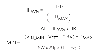
where a tolerance parameter (LTOL = 0.2) has been applied on the minimum inductance’s nominal value, expressed in Henries.
Using an efficiency of η = 90%, VIN_MIN = 4.5V and VLED = 30V, the calculated LMIN is 0.85µH. Converting this value to a greater standard value, a value of 2.2µH can be used for L1.
The current rating of the chosen inductor must be greater than its peak current (ILP), given by:

The recommended saturation current limit of the selected inductor should be 10% higher than the inductor peak current.
Output Capacitors
In the boost converter topology, the output capacitor supplies the load current when the switching MOSFET is on. The function of the output capacitor is to reduce the converter output ripple to acceptable levels. The entire output-voltage ripple appears across the constant-current sink outputs because the LED-string voltages are stable due to the constant current.
The ESR, ESL, and the bulk capacitance of the output capacitors contribute to the total output voltage ripple, which should be limited to 250mV peak-to-peak to get a stable output current. In most applications, using low-ESR ceramic capacitors can dramatically reduce the output ESR and ESL effects. To reduce the ESL and ESR effects, connect multiple ceramic capacitors in parallel to achieve the required bulk capacitance. To attenuate audible noise during PWM dimming, the number of ceramic capacitors on the output is usually minimized. In this case, an additional electrolytic or aluminum organic polymer capacitor provides most of the bulk capacitance. Alternatively, low acoustic noise ceramic capacitors can be used. A total output capacitance of 30µF is a good starting value.
Output Diode
A Schottky diode with low reverse-recovery losses should be selected to reduce the MOSFET switching losses and to avoid increased EMI. The reverse voltage rating of the diode should be 20% higher than the maximum boost-converter output voltage and its current rating greater than that shown below:
ILAVG x (1 - DMAX ) x 1.2
where the 1.2 factor was included for margin.
NMOS Input Protection FET
An external nMOSFET can be used to disconnect the boost output from the battery in the event of an output overload or short condition. The maximum value of the nMOSFET gate threshold voltage must be lower than 4V for reliable operation.
If this protection is not necessary and there is no need for the nMOSFET, the NGATE pin must be left unconnected and the CP_DIS bit in register DISABLE must be set to 1.
Feedback Resistor-Divider
The overvoltage-protection threshold is used to limit the output voltage through a voltage-divider network connected between the converter output, the BSTMON input, and GND. In the event that the BSTMON voltage exceeds 0.95V, the internal switching MOSFET will be turned off, preventing the boost output voltage from going higher.
The overvoltage-protection threshold at the DC-DC converter output is determined using the following equation:

where 0.95V (typ) is the overvoltage threshold on BSTMON.
VBSTMON is the maximum voltage the boost converter can produce and should be set according to the following formula:
1.1 x (VLED + 0.875)< VBSTMON < 2 x (VLED + 0.55)
R6 and R7 must be selected such that the output voltage does not exceed its absolute maximum rating (40V) while respecting the formula above. By selecting R6 = 360kΩ and R7 = 10kΩ, the following value for VBSTMON is obtained:
VBSTMON = 0.95V × 37 = 35.15V
Feedback Compensation
It is known that the switching converter’s small-signal-transfer function has a right-half-plane (RHP) zero in the boost configuration if the inductor current is in continuous-conduction mode. Its frequency is given by the following formula:

The switching converter small-signal transfer function also has an output pole. The effective output impedance, together with the output filter capacitance (COUT), determines the output pole frequency (fp1) as follows:

Loop compensation is guaranteed by a Type II transconductance amplifier (error amplifier) which characterizes the closed-loop response.
The goal of loop compensation is to ensure that there is less than 180° of phase shift for loop gains > 0dB (and adequate phase margin). The error amplifier adds a zero-frequency pole due to the integrating effect of CCOMP which allows it to roll off the loop gain to 0dB with a -20dB/decade slope (after the dominant pole and well before the effects of the RHPZ).
It is generally recommended that the closed-loop gain crossover frequency, fC, is limited to at least one-fifth of the RHPZ frequency to obtain an acceptable phase margin (higher than 45°). The compensation zero, fzEA, should be placed at one-fifth of the target crossover frequency at least, which is at approximately fRHPZ/25.
The optimum value of RCOMP needed to fix the total loop gain at fp1, so that the total loop gain crosses 0dB with -20dB/decade slope at 1/5 the RHPZ frequency, is given by:
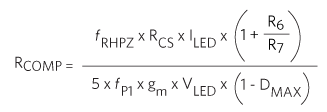
where gm = 600µS and RCS= 0.066Ω.
The value of CCOMP can then be calculated as shown below:

The higher in frequency that the loop gain stays above zero before crossing 0dB, the faster the loop response is and, therefore, the lower the output voltage drops during a load step. Lowering RCOMP, while keeping fzEA ≈ fC/5, increases the phase margin without significantly changing the gain and therefore increases the time it takes for the output voltage to settle following a load step.
Given the design parameters and the previously calculated component values:
fRHPZ = 71.82kHz
fp1 = 169.8Hz
RCOMP = 43.72kΩ
CCOMP = 1.27nF
RCOMP = 20kΩ and CCOMP = 3.3nF can be selected as standard commercial values in this numerical example.
Thermal Considerations
The on-chip power dissipation of the MAX25512 comprises four main factors: current-sink power loss (PSINK), quiescent power loss (PQ), power loss related to the RDS(ON) of the internal MOSFET (PRDS_ON), and power loss related to switching activity of the internal MOSFET (PSW). The four factors can be calculated as follows:
PSINK = 0.875V x ILED
PQ = 1.3mA x VIN_MIN
PRDS_ON = DMAX x IL2AVG x rDS_ON_MAX
PSW = 0.5 x VLED x ILED x fSW x tR/F
tR/F in the last equation is the rise/fall time of the boost converter switching node approximated to 6ns.
The total power dissipation (PTOT) is obtained by adding the values calculated above. The junction temperature (TJ) at the maximum ambient temperature can then be calculated as follows:
TJ = TA + PTOT x θJA
where TA is the ambient temperature and θJA is the junction-to-ambient thermal resistance of the package (36°C/W on a four-layer board). The junction temperature must not exceed +150°C.
Considering two applications with VIN_MIN = 5.5V (η = 90%) and VIN_MIN= 9V (η = 92%), respectively, by inserting into the power loss equations, the design parameters and values calculated using the formulas in the previous sections, the sum of the power loss factors gives:
PTOT = 1441.87mW (VIN_MIN = 5.5V)
PTOT = 777.87mW (VIN_MIN = 9V)
The maximum junction temperature at an ambient temperature of 25°C is shown in the following equations for the two cases:
TJ = 25 + 1441.87 x 10−3 x 36 = 76.9°C
TJ = 25 + 777.87 x 10−3 x 36 = 53°C
I2C Interface
The MAX25512 includes an I2C 2-wire serial interface consisting of a serial-data line (SDA) and a serial-clock line (SCL). SDA and SCL facilitate communication between the IC and the master at clock rates up to 400kHz. The master, typically a microcontroller, generates SCL and initiates data transfer on the bus.
| Device Address | 8-bit Write Address | 8-bit Read Address |
| A6 A5 A4 A3 A2 A1 A0 | 0 x 44 | 0 x 45 |
| 0 1 0 0 0 1 0 |
A master device communicates with the MAX25512 by transmitting the correct Slave ID with an appended R/W bit, followed by the register address and data word (for a write transaction only). Each word transmitted over the bus is 8 bits long and is always followed by an acknowledge clock pulse.
The IC's SDA line operates as both an input and an open-drain output. A pullup resistor greater than 1kΩ is required on the SDA bus. In general, the resistor should be selected as a function of bus capacitance such that the rise time on the bus is not greater than 120ns. The IC's SCL line operates as an input only. A pullup resistor greater than 1kΩ is required on SCL if there are multiple masters on the bus, or if the master in a single-master system has an open-drain SCL output. In general, for the SCL-line resistor selection, the same recommendations apply as for the SDA. Series resistors in line with SDA and SCL are optional. The SCL and SDA inputs suppress noise spikes to ensure proper device operation even on a noisy bus.
Conclusion
TFT-LCDs dominate the automotive display market. It is estimated that there are now up to 12 displays being used in each automobile. These solutions require higher current with precision, flexibility, and small overall solution size and cost to meet increasingly stringent system requirements. In this design solution, we demonstrated how to design an LED backlight power management circuit considering common TFT-LCD designs. This design solution also detailed how the MAX25512 not only provides a small and compact solution size, but is very easy to use, is easily configurable, and has different preprogramming options.


