Flexible Power Supply Sequencing and Monitoring
Introduction
The LTC2924 is a complete power supply sequencer and supervisor solution for multivoltage-rail systems, such as telecommunications equipment, memory modules, optical systems, networking equipment, servers, and base stations. The FPGAs and other digital ICs used in these applications require multiple voltage rails that must start up and shut down in a specific order, otherwise the ICs can be damaged. The LTC2924 is a simple and compact solution to power supply sequencing in a 16-pin SSOP package (see Figure 1).
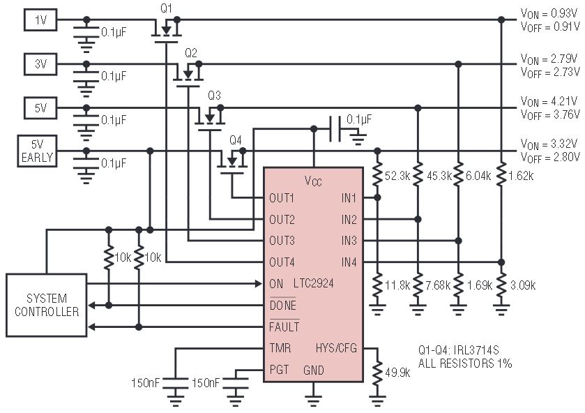
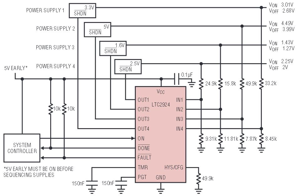
Figure 1b. Similar application to Figure 1a, but control is via the converter shutdown pins.
Sure, alternative sequencing solutions are available, but few, if any, can match the ease-of-use, space-saving design, flexibility, and cost effectiveness of the LT2924. For instance, solutions that use discrete components incur a challenging and time-consuming design effort to interface with the digital system, and consume a significant amount of board real estate. Another option, an integrated power supply sequencer, is more expensive and consumes more board space than any LTC2924-based solution, and may require proprietary software and the programming of complicated digital registers. Neither of these options comes close to offering the flexibility across applications that the LTC2924 does. It can be used out-of-the-box, with a few external components, to sequence and supervise just about any type of power supply, converter, or power module.
How it Works
Four power supplies can be easily sequenced using a single LTC2924, and multiple LTC2924s can be just as easily cascaded to sequence any number of power supplies. With slightly reduced functionality, six power supplies can be sequenced with a single LTC2924 (see Figure 5 and “Sequencing Six Supplies with a Single LTC2924” in this article).
The LTC2924 controls the start-up and shutdown sequence, and ramp rates, of four power supply channels via output pins (OUT1–OUT4). Each OUT pin uses a 10μA current source connected to an internal charge pump and a low resistance switch to GND. This combination makes the outputs flexible enough to connect them directly to power supply shutdown pins, or to external N-Channel MOSFET switches. Figure 1a illustrates a typical application for the LTC2924 where four supplies are sequenced using external N-channel MOSFETs, and Figure 1b shows a comparable circuit with four power supplies sequenced using their shutdown pins.
The LTC2924’s internal charge pump allows the designer to use N-channel MOSFET switches, which are typically lower in cost and RDS(ON) than comparable P-channel MOSFETs. The internal charge pump provides a gate voltage of VCC + 5V, which fully enhances an external logic level MOSFET. The 10μA pull up current source on the output pin allows the implementation of a soft-start (ramped voltage start-up) by including an optional capacitor between the gate of the MOSFET and ground.
The LTC2924 monitors the output voltage of each sequenced power supply via four input pins (IN1–IN4). These inputs use precision comparators and a trimmed bandgap voltage reference to provide better than 1% accuracy. The power ON and power OFF voltage thresholds are set using resistive dividers for each of the four channels. The the power ON threshold and the power OFF threshold is individually selectable on a channel by channel basis. (see “Selecting Resistors for the Turn On and Turn Off Voltage Thresholds” in this article for details).
The LTC2924 timer pin (TMR) is used to provide an optional delay between the completion of start-up of one supply, and the start-up of the next power supply. The delay time is selected by placing a capacitor between the TMR pin and ground (delay = 200uS/nF), whereas floating the TMR pin removes any delay. The start-up delay can be different than the shut-down delay. Figure 2 shows a simple circuit where the shut-down delay is half the start-up delay.
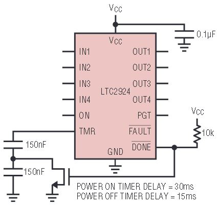
Figure 2. Power ON sequence timer delay longer than power OFF sequence timer delay.
The LTC2924 also includes a power good timer (PGT). The LTC2924 starts the PGT as each individual power supply is enabled. If any power supply fails to reach its nominal specified voltage within the allotted time interval, a Power ON fault is detected. The PGT is enabled for the time interval set by a capacitor between the PGT pin and ground. The PGT is disabled by grounding the PGT pin.
The LTC2924 DONE pin is used to report the status of the power sequencing to a system controller. The LTC2924 signals the completion of an entire 4-channel Power ON sequence by pulling down the open-drain DONE pin. The completion of a Power OFF sequence is signaled by releasing the DONE pin.
The LTC2924 open drain FAULT pin is bi-directional. The LTC2924 signals a FAULT condition to a system controller by pulling this pin down. Conversely, a system controller can trigger the immediate, simultaneous turn off of all sequenced power supplies by pulling down the FAULT pin. This may be used as an alternate way of powering down a system.
Selecting Resistors for the On and Off Voltage Thresholds
Each of the four channels of the LTC2924 can have its own values of VON, the turn on voltage threshold, and VOFF, the turn off voltage threshold. Setting the voltages is easy—only two resistors are required at the input pin of each channel, and choosing the resistor values is simple, as described here.
Refer to Figure SB1. The first step is to select a hysteresis current (IHYS). This current is used by all four channels, and is programmed by one resistor, RHYS on the HYS/CFG pin in Figure SB1. The IHYS current is switched in to each IN1-4 pin when each channel is ON. Unless the LTC2924 is being used in a very low power system use 50μA for IHYS. Calculate RHYS from IHYS by the following:


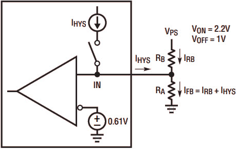
Figure SB1. Designing IHYS feedback resistors.
That leaves the two resistors for each channel. For each sequenced power supply, choose VON, the voltage at which power is considered on during a start up sequence, and VOFF, the voltage at which power is considered off during a shut down sequence. Referring to Figure SB1, RB is the resistor connected between the sequenced power supply and the IN pin and RA is connected between the IN pin and ground. Each resistor can be then calculated by:

This allows the hysteresis band for each channel to be individually tailored.

Perform this simple calculation for each channel. For example, if:

Place this resistor between the HYS/CFG pin and ground.
With VON and VOFF voltages:

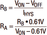
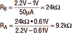
Repeat the last four calculations for the remaining three channels.
Sequencing and Monitoring with the LTC2924
The LTC2924 ON pin is used to initiate Power ON and Power OFF sequences. The ON pin uses the same precision comparator circuits as the four IN pins. The ON pin can either be controlled by a logic level from a system controller, or it can be used to sense the voltage level of an un-sequenced power supply. When the voltage at the ON pin rises above 0.61V, the LTC2924 initiates the Power ON sequence. At this point the first timer interval occurs. Upon completion of the timer interval, the OUT1 pin is pulled high with its 10μA current source connected to the internal charge pump voltage. Once the voltage of the first power supply reaches its preset threshold—as monitored at the IN1 pin—and after the second delay, the OUT2 enable signal is generated for the subsequent power supply. The sequence repeats until the forth channel is powered up. At this time the DONE pin pulls low to signal the completion of the Power ON sequence.
The LTC2924 then enters supervisor mode. The LTC2924 continues to monitor the power supply voltages (at the IN1–IN4 pins). If any of the power supplies fall below the designed OFF voltage, the LTC2924 indicates a fault and all of the OUT pins are pulled low. The fault condition is communicated to the system controller by pulling the FAULT pin low.
The Power OFF sequence can be initiated in one of two ways. To turn off all of the power supplies simultaneously, the system controller can pull down on the FAULT pin. To sequence off the power supplies, the system controller pulls the ON pin voltage low. The Power OFF sequence is executed in the reverse order of the Power ON sequence, with the supply that was powered up last is powered down first, and the supply that was powered up first is powered down last.
Figure 3 illustrates the power supply up and down sequences for a typical 4-supply application. After the ON pin goes low, the timer delay occurs before the OUT4 pin is pulled low. When the power supply goes below its turn off voltage, there is another timer delay. The sequence repeats until the final power supply has powered down. The LTC2924 signals the end of the Power OFF sequence by releasing the DONE pin.
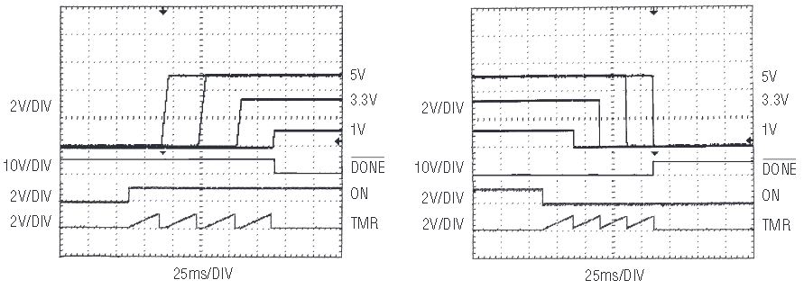
Figure 3. Power up and power down sequences for a typical 4-supply circuit.
Cascading the LTC2924 for Eight Supplies and Up
Two or more LTC2924s can be cascaded to fully sequence eight or more supplies. The smart configuration logic in the LTC2924 makes the job of cascading multiple LTC2924 ICs easy. Figure 4 shows three devices configured to sequence 12 supplies. To set the sequence of each of the LTC2924 ICs, the HYS/CFG, DONE, and ON pins are connected as shown. See the LTC2924 data sheet for operational details. To sequence more than 12 power supplies, simply add more LTC2924 ICs in the middle, or 2nd position, in Figure 4. To sequence up to eight power supplies remove the LTC2924 in the middle position.
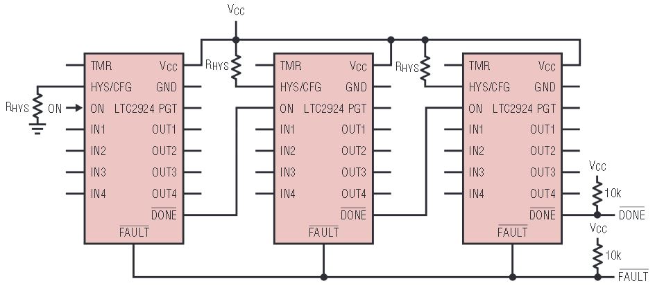
Figure 4. Cascading LTC2924 ICs to sequence 12 power supplies.
Sequencing Six Supplies with a Single LTC2924
Figure 5 shows how to sequence six supplies with one LTC2924. When the system controller releases the TURN OFF node, the first power supply turns on. The ON pin is tied to the output of the first power supply. Once this power supply is powered on, the LTC2924 sequentially starts up power supplies 2 through 5. When the DONE pin is pulled low after the 5th power supply powers ON, the inverted signal allows the 6th power supply to turn on. This inverter can be implemented with a single transistor. The system controller can power off all six power supplies simultaneously by pulling the TURN OFF node low.
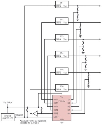
Figure 5. A 6-supply sequencer.
Delayed Remote Sensing
Remote sensing is a common configuration in high current applications. Parasitic resistances in the power supply path coupled with high DC currents can result in unacceptable DC voltage drops. The sense pin of a power module is designed to regulate the DC voltage at a point in the power distribution circuitry beyond the parasitic resistance to compensate for the I • R voltage drop. The output voltage of the power module is raised until the desired voltage is reached at sense point.
The problem with this feedback scheme is that many power modules have unalterable maximum output voltages, which, if exceeded, cause the power supply to shut down. This limits the amount of voltage correction available to compensate for parasitic I • R voltage drops. Transient start-up inrush currents, caused by charging power supply bypass capacitors, often exceed the normal DC currents and create a large I • R voltage drop across the parasitic resistance. If the sense pin is connected to the remote sense point, the power module tries to compensate for the additional voltage drop by raising its output voltage, possibly higher than its set maximum. This, off course, causes the power module to shut down before it has even finished starting up. This problem can be avoided by delaying remote sensing until the inrush currents have diminished.
Figure 6 shows how delayed remote sensing can be achieved with the LTC2924. In Figure 6, Channel 1 is a DC-DC converter that receives its input power from the power module. Channel 2 switches on the power module that is being remote sensed and Channel 3 is the remote sense enable. As Figure 7 shows, when the LTC2924 ON pin is pulled HIGH the Power ON sequence is initiated. After the time delay is executed, the DC-DC converter connected to OUT1 is enabled. When the output voltage level on this supply goes above the user-configured threshold voltage the second delay is triggered, and then Q1 is turned on. When the output voltage reaches 4.64V, the 3rd output is enabled after another delay. This enables the remote sensing of the power supply after the initial transient currents have subsided. As Figure 7 illustrates, the output voltage of the power supply increases to the desired level after the remote sensing is enabled.
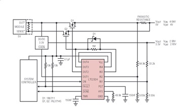
Figure 6. Delayed remote sensing.
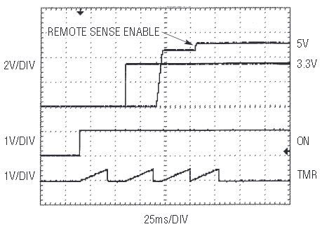
Figure 7. Delayed remote sensing power up sequence.
Power Supply Fault Monitoring and Reporting
The LTC2924 has the capability to monitor the supply levels and report any fault conditions that are detected. If one or more of the following errors are detected, the LTC2924 immediately turns off all supplies and signals a FAULT condition by pulling the FAULT pin low. The LTC2924 can detect:
- Power ON and Power OFF sequence errors: The LTC2924 keeps track of each of the supplies during the Power ON sequence, during the time the power is on, and during the Power OFF sequence. If at any time a power supply output goes low when it should be high, a fault is generated.
- System controller command errors: The ON pin is the input signal provided by the system controller to direct the LTC2924 power sequencing. By taking this pin HIGH, a Power ON sequence is initiated. Until all the power supplies are powered on, the ON pin must remain HIGH. During the Power OFF sequence the voltage on this pin must remain below 0.61V. If these conditions are not maintained during the Power ON or Power OFF sequencing, the LTC2924 indicates a fault condition.
- Power Good Timer (PGT) Power ON timeout failures: The PGT is enabled with a single capacitor at the PGT pin with a transfer function of 200μs/nF. If a supply that is being sequenced ON does not reach the desired voltage level within the time set by the PGT, a fault is generated.
- External faults: The FAULT pin can also be used as an input. Pulling the FAULT pin low causes the LTC2924 to turn off all power supplies and abort any sequence in progress.
If any of the conditions above are met, the LTC2924 pulls all of the OUT pins low causing all power supplies to turn OFF. The FAULT pin is also pulled low to report the event to a system controller. The TMR pin is also pulled high if the fault condition was generated internally. The fault condition is not reset until all of the IN pins and the ON pins are below 0.61V.
Conclusion
The LTC2924 fits into a wide variety of power supply sequencing and monitoring applications. With very few external components and a 16-pin narrow SSOP, an LTC2924 based sequencing solution requires very little board space.
The power supply enable pins require no configuration by the designer, yet are versatile enough to directly drive shutdown pins or external N-channel MOSFETs. Soft start of power supplies can be achieved simply by adding a capacitor. If the sequencing of more than four power supplies is required, the LTC2924 can be cascaded to sequence a virtually unlimited number of power supplies. With the addition of a single capacitor, a timer can be enabled and programmed. Adding one more capacitor programs and enables a Power Good Timer (PGT). Power supplies can be turned off in the reverse order of turn on, or they can all be turned off at the same time.
Tailoring the LTC2924 to a specific application requires no software and designs can be fine tuned during system integration simply by changing resistor and capacitor values. Ease of design, low component cost, and a small footprint make the LTC2924 an excellent choice for power supply sequencing and monitoring.


