Dual Output Monolithic Supply with Integrated 3A Power Switches and Operation to 2.5MHz in a 7mm × 4mm DFN
Dual Output Monolithic Supply with Integrated 3A Power Switches and Operation to 2.5MHz in a 7mm × 4mm DFN
2012年04月01日
There is no shortage of ICs to help designers build switching DC/DC switching power supplies. Choices range from versatile controllers requiring a number of external components, to fully integrated, monolithic solutions that benefit from a low external parts count to minimize overall solution size. The LT8582 dual-channel converter offers the versatility of a controller IC in a complete, monolithic dual-channel solution.
The LT8582 integrates two complete, independent converters, including high power 3A, 42V power switches. It can operate up to 2.5MHz, and with its tiny 7mm × 4mm DFN package, fits into the smallest spaces. It includes several features that give designers the ability to optimize the converter, such as soft-start, single-pin feedback, single-resistor frequency setting, master/slave power switches, separate maximum commanded and fault current limits, external PFET control for output or input disconnect, FAULT protection, PG pin for power supply sequencing, and CLKOUT signal for out-of-phase synchronizing and die temperature monitoring.
Flexibility and Simplicity
Each channel of the LT8582 can be independently configured in a boost, SEPIC, inverting or flyback topology. Figure 1 shows a few common combinations that could be used in commercial or industrial applications, such as local power supplies, LCD/E-ink displays, and engine control units (ECU).
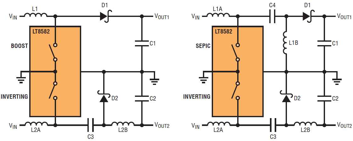
Figure 1. Common dual power topology combinations.
The LT8582 is rugged, with solid performance. Even with all of its advanced features, it is easy to use—designers can choose to apply features to fit a variety of applications. Its wide input operating voltage of 2.5V to 22V, and the 3A, 42V switches on each channel add to the versatility of the chip.
High Switching Frequency
The LT8582’s constant frequency oscillator, programmable from 200kHz to 2.5MHz using one resistor, employs frequency foldback to better control the inductor current during converter start-up. This wide frequency range allows the switching noise to be placed so that sensitive frequencies are avoided. While lower switching frequencies offer better efficiency, higher switching frequencies help reduce the size of passive components. The switching frequency can be synchronized to an external clock by connecting a clock signal to the SYNC pin. Grounding the SYNC pin enables the internal oscillator.
CLKOUT Pin, Synchronizing and Temperature Monitoring
The LT8582 has two CLKOUT signals, one for each channel. CLKOUT for channel 1 has a fixed 50% duty cycle and is 180° out of phase with the power switch. This can be used to sychronize channel 2 antiphase to channel 1, reducing the converter’s overall input current ripple. The CLKOUT signal for channel 2 features a duty cycle that varies with die temperature (3% per 10°C) and is in phase with the power switch. This can be used for monitoring the die temperature.
Fault Protection and the Gate Pin
The LT8582 has internal circuitry to detect switch overcurrent, VIN overvoltage and die overtemperature (> ~165°C). The chip’s GATE pin is a pull-down current source and can control an external PFET during the fault. The external PFET can disconnect the input or the output, as shown in Figure 2.

Figure 2. Controlling external PFETs for input disconnect (left) and output disconnect (right).
When a fault is detected, the LT8582 stops switching and the GATE pin becomes high impedance. The external PFET is then turned off by the external RGATE resistor. The RGATE resistor must be selected so that sufficient VGS is available for the PFET to fully enhance into triode under normal operation. When the fault is removed, the LT8582 enters a timeout period, allowing components to cool down before a restart sequence begins.
Reverse input voltage protection and output short circuit protection can be achieved, as shown in Figure 3, using two external PFETs and the GATE pin. At start-up, the channel’s supply voltage is provided through the body diode of M2 while M1 keeps the power path disconnected. When the GATE pin is pulled down, both PFETs turn on. If the input voltage is reversed, the channel and the power path are disconnected from the input supply by M2. If the output is shorted, the power path is disconnected from the input supply by M1. The GATE pin can be left floating when not in use.
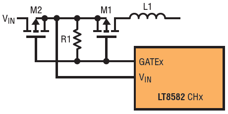
Figure 3. Reverse battery and output short protection.
Another use of the GATE pin is to limit the converter start-up current. During start-up, the GATE pin current increases linearly with SS pin voltage, to a maximum current of ~1mA when the SS voltage exceeds 500mV. This allows the external PFET to slowly turn on and gradually ramp up the output voltage. Together with frequency foldback and soft-start, this feature allows converter start-up to be very smooth, even for hot-plug events.
Figure 4 illustrates how the GATE pin provides short-circuit protection for a boost converter. The circuit produces ±12V output from 5V input supply by utilizing channel 1 of the chip as a boost converter and channel 2 as a dual inductor, inverting converter.
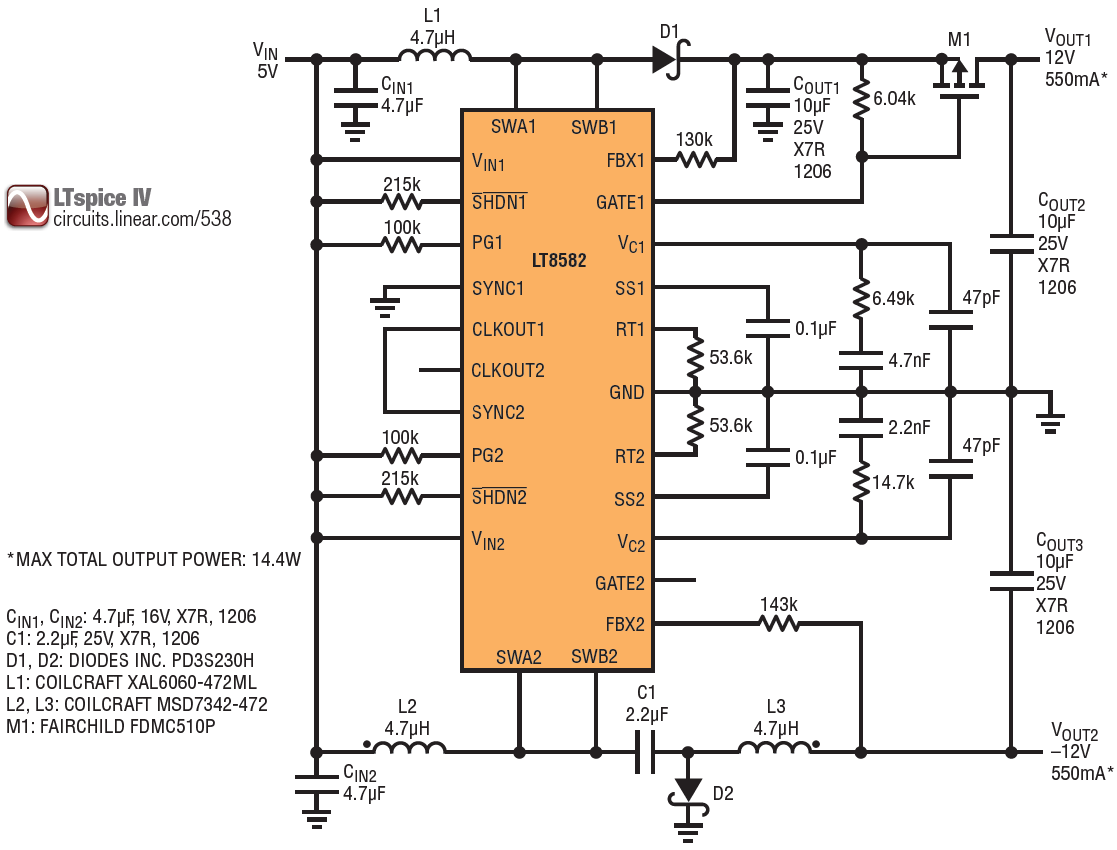
Figure 4. A 1.5MHz +5V to ±12V dual converter using one LT8582.
A common weak point of the boost topology is that it has a direct DC path from input to output through the inductor and diode. An output short can result in an uncontrolled increase of current through the converter, likely destroying one or more components in the DC path and the power switch if it switches during this time. The LT8582 addresses this issue by disconnecting the DC path if the part senses an overcurrent condition.
For the dual inductor inverting and SEPIC topologies, because of the series capacitor in the power path, there is no direct DC path between input and output and the external PFET is not required.
The circuit in Figure 4 is running at a high switching frequency of 1.5MHz. If thermal issues arise, using larger ground planes and better air flow helps remove extra heat.
Master/Slave Power Switch
Each channel of the LT8582 incorporates a master and a slave switch, which are rated at 1.7A and 1.3A, respectively. The switches are driven in phase and only the current through the master switch is sensed by the internal current comparator. Normally, these switches are tied together; when separated, they can be used for building high voltage charge pumps, as shown in Figure 5. The charge pump circuit generates output voltages that are higher than what the IC can tolerate.
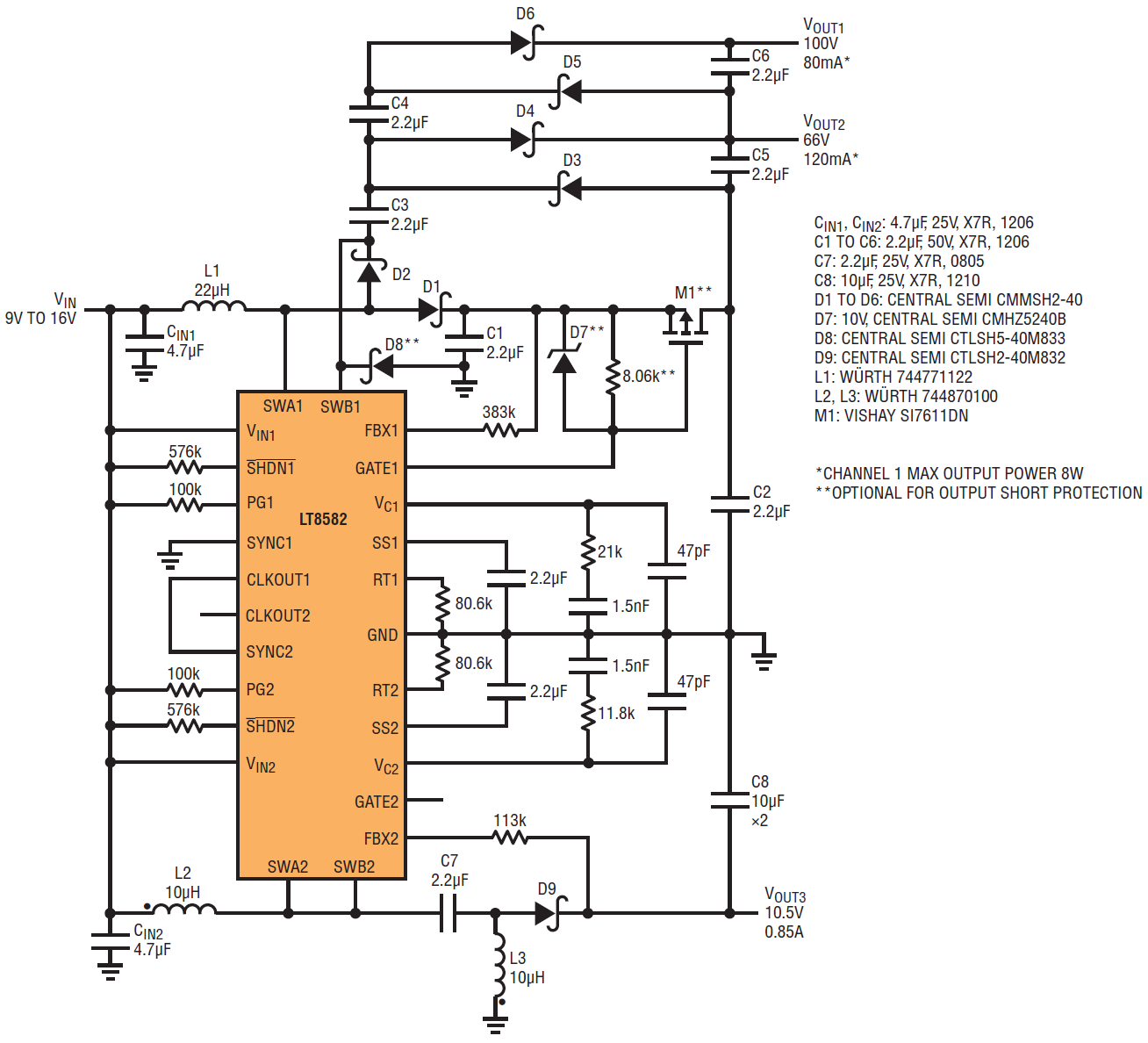
Figure 5. High voltage VFD and filament bias supplies.
The first stage of the charge pump circuit is based on boost topology and uses the channel’s master switch. The channel’s slave switch is used to drive the other charge pump stages, multiplying the output voltage of the boost stage. The benefit of this configuration is that the master switch is immune from capacitive current spikes, allowing the LT8582 to sense the inductor current distinctly. Moreover, the charge pump diodes do not need series resistors that are typically used to limit the capacitive current spikes.
The high output voltage can be used for low current loads such as vacuum fluorescent displays (VFDs). In this case, the second channel of the LT8582 can be configured as a SEPIC converter to bias the filament of the VFD. Here, the master and slave switches of channel 2 can be tied together to increase output current. Figure 6 shows the efficiency of the charge pump circuit at various power levels.
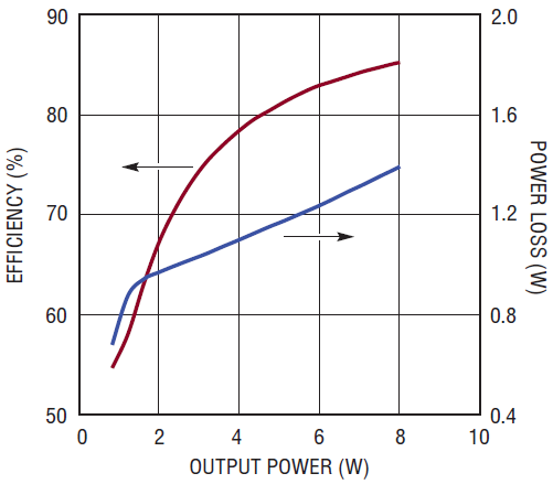
Figure 6. Charge pump efficiency vs output power.
Fault and VC Current Limits
The LT8582 has two distinct current limits: the VC current limit, which is the maximum current that can be commanded, and the FAULT current limit, which is the maximum current in case of converter overcurrent. The FAULT current limit is internally set higher than the VC current limit. When the FAULT current limit is reached, the chip goes into fault mode and stops switching. However, when the VC current limit is reached, the chip reduces the switch duty cycle, reducing the output voltage.
The VC current limit feature can be used in situations where the load voltage may be low for an extended period of time, such as when charging supercapacitors. Figure 7 demonstrates how the VC current limit along with the GATE pin can be used to build a backup power supply using one LT8582 and a bank of four supercapacitors.
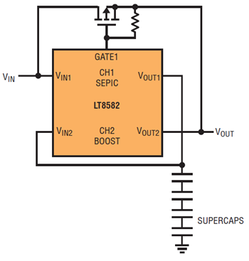
Figure 7. Charging/discharging supercapacitors in a backup power supply.
The actual circuit is shown in Figure 8. Here, channel 1 of the LT8582 is configured as a SEPIC converter and is used to charge the supercapacitor bank when VIN is present. At this time, the GATE pin of channel 1 is enabled and the external PFET provides a path for the load current from the input to the output. Once the input supply is disconnected, channel 2 of the LT8582 which is configured as a boost converter, provides voltage to the load without any delay, while the external PFET disconnects the input from the output, preventing energy from going back into VIN.
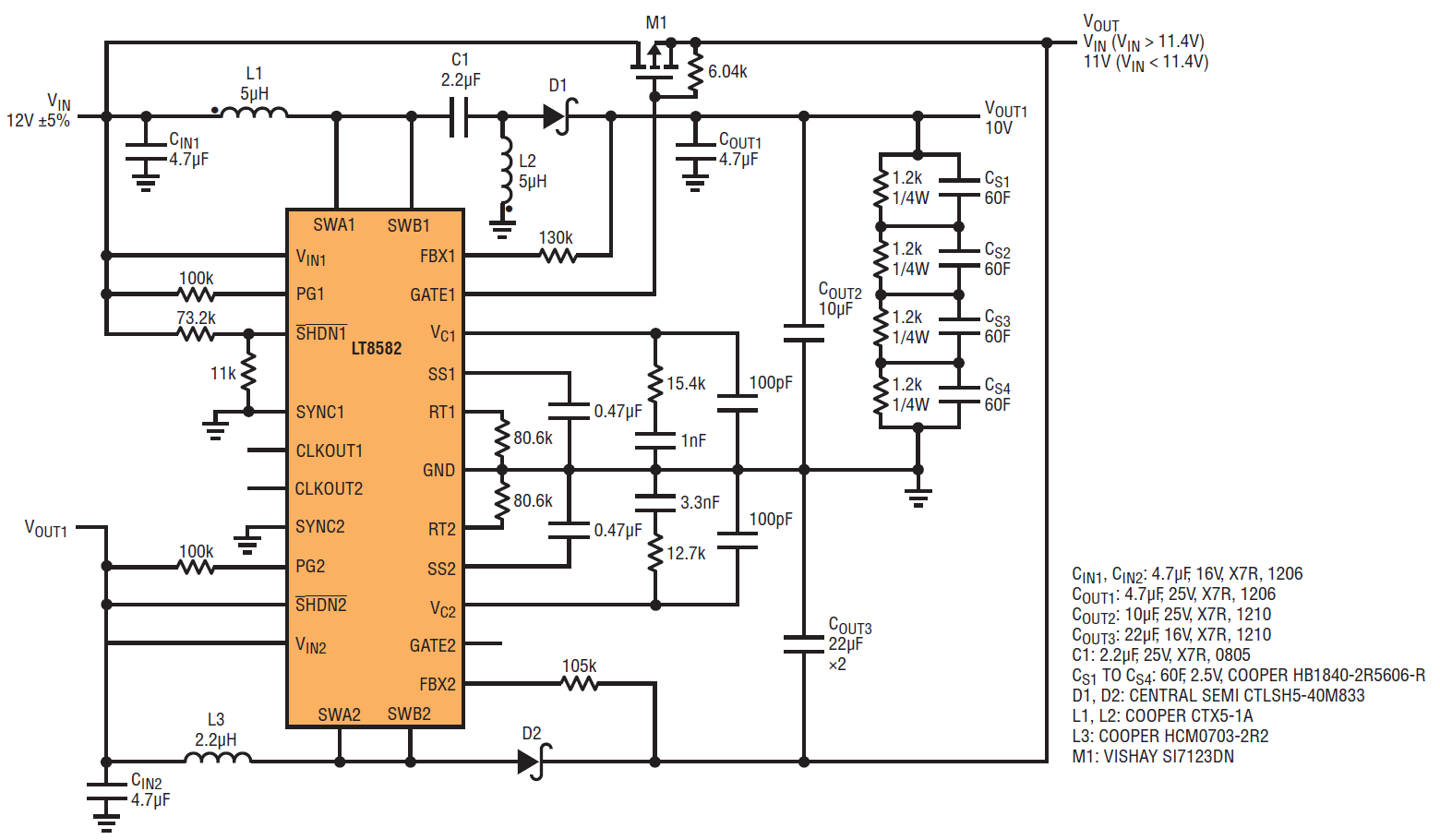
Figure 8. Backup power supply using supercapacitors.
The complete backup power supply circuit is shown in Figure 8. With the component values shown, the supercapacitor bank is charged to 10V when VIN is above ~11.4V. Once VIN falls below ~11.2V, the circuit holds up VOUT at 11V for about 90 seconds with 500mA of load current. The waveforms of interest during charging/discharging the supercapacitors are shown in Figure 9.
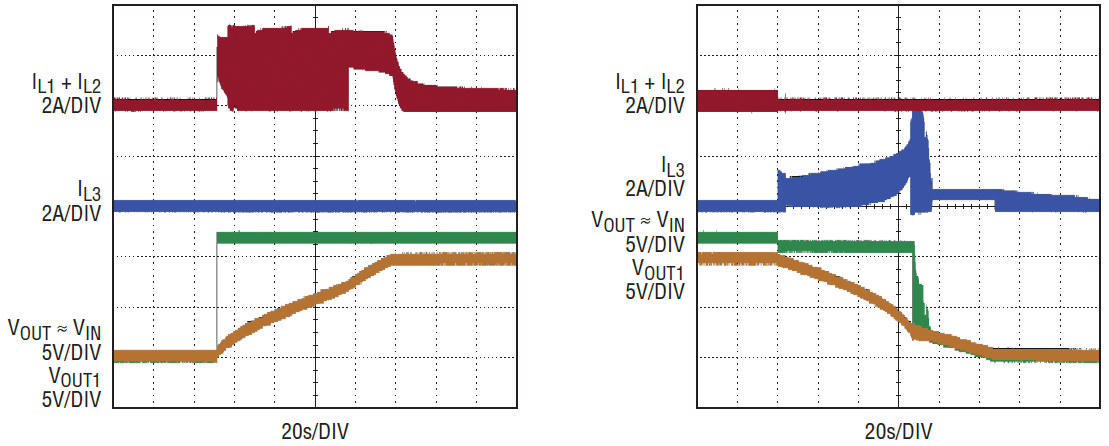
Figure 9. Waveforms of interest during charging (left) and discharging (right) the supercapacitors.
PG Pin and Event-Based Sequencing
The PG pin is an open drain active high pin that indicates the output voltage is close to regulation. For most applications this corresponds to an output voltage 8% from the target output voltage. The SHDN pin is used to enable/disable the channel. Driving the SHDN pin to ground disables the channel while driving SHDN above 1.3V enables the channel.
Figure 10 shows how these two pins can be used to turn on power supplies in sequence as may be required in systems with multiple voltage levels. When channel 1’s output voltage is close to regulation, the PG pin of channel 1 releases channel 2’s SHDN pin, which enables channel 2. To ensure that the status of channel 1’s PG pin is valid while it is being sensed by channel 2, channel 1 has to become active first, i.e., VIN1 UVLO should be set lower than VIN2 UVLO. To provide a global shutdown signal for the system, the SHDNSYS signal drives two NFETs that disable both channels when it is high.
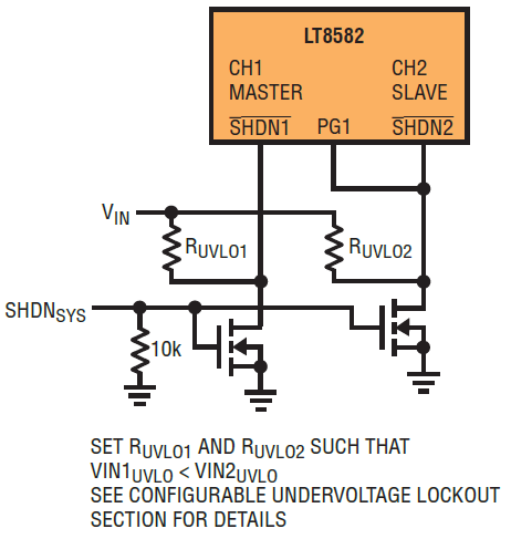
Figure 10. Sequenced power supplies.
The complete circuit diagram and start-up waveforms are presented in Figures 11 and 12.
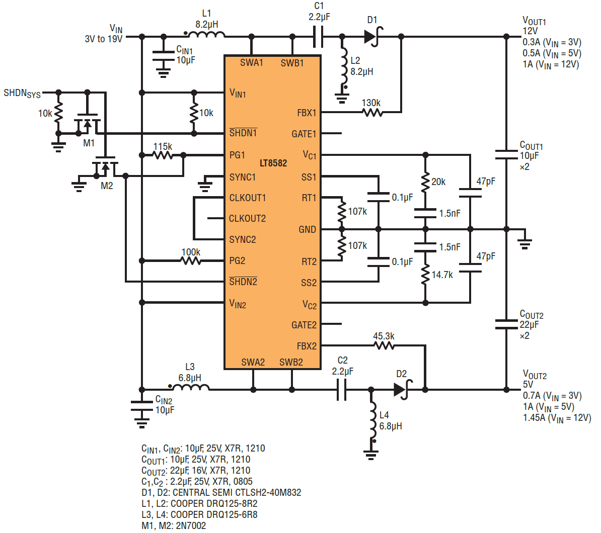
Figure 11. Sequenced 12V and 5V dual outputs.
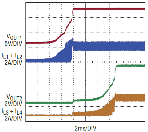
Figure 12. Start-up waveforms at VIN = 12V.
FB Pin and Single Resistor Voltage Feedback
The LT8582 needs only one feedback pin for both positive and negative output voltages. In addition, only one external resistor from VOUT to FB is required to set the output voltage. The internal feedback circuitry automatically selects the correct reference voltage, 1.204V or 7mV for topologies with positive or negative outputs, respectively.
This feedback structure can be used to design simple tracking power supplies without using a tracking controller chip. As shown in Figure 13, only one extra resistor connected between the two feedback pins of LT8582 is needed for this.
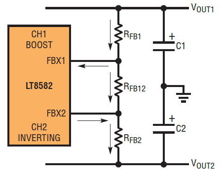
Figure 13. Tracking power supplies using one extra resistor.
RFB1, RFB12 and RFB2 form a resistor voltage divider. The more current through them, the better the tracking. Thus, the current through the connecting resistor RFB12 must be relatively higher than the FB1 and FB2 currents, so:

After selecting RFB12, the feedback resistors RFB1 and RFB2 can be calculated as follows:
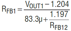
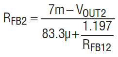
For the circuit shown in Figure 14, plotting the output voltages vs load currents yields Figure 15.
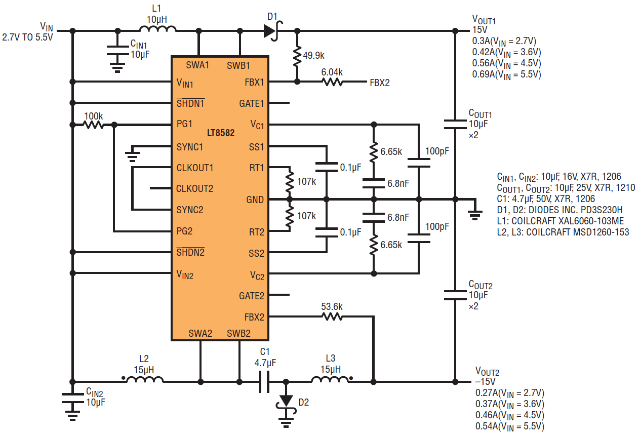
Figure 14. Dual tracking power supplies using one LT8582.
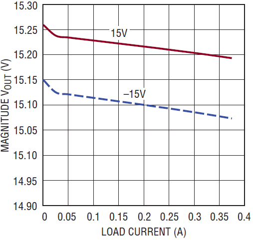
Figure 15. Tracking output voltages vs load current (load between the two outputs).
Conclusion
The LT8582 is a dual independent monolithic converter with two 3A, 42V power switches. In addition to popular features such as soft-start, single-pin feedback and single-resistor oscillator, it includes unique features such as the master/slave power switches, separate maximum commanded and fault current limits, external PFET control for output or input disconnect, FAULT protection, PG pin for power supply sequencing, and CLKOUT signal for out-of-phase synchronizing and die temperature monitoring. These features enable the LT8582 to be used in a variety of applications, from typical dual rail voltage regulators to supercapacitor backup supplies.
The LT8582 is easy to use and robust. Because of its high switching frequency and monolithic structure, it can be used to fit power converters into the tightest spaces. The LT8582 is available in a tiny 24-pin 7mm × 4mm DFN package.


