Dual, 1.4A and 800mA, Buck Regulator for Space-Sensitive Applications
Dual, 1.4A and 800mA, Buck Regulator for Space-Sensitive Applications
著者
Scott Fritz
2005年09月01日
Introduction
The evolution of cell phones, PDAs, palmtop PCs, digital cameras, PC cards, wireless and DSL modems is one of squeezing an increasing number of features in ever-smaller devices. As features increase, so do the number of required power supplies. The problem is how to fit more supplies in less space. There are a number of solutions, including: increasing the switching frequency (allowing the use of smaller and less costly capacitors and inductors), integrating the switcher MOSFETs, or combining multiple switchers into a single package. The LTC3417 combines all of these.
A Small Package Loaded with Features
The LTC3417 is a dual synchronous, step-down, current mode, DC/DC converter designed for medium power applications. It operates from an input voltage between 2.25V and 5.5V and switches at up to 4MHz, making it possible to use capacitors and inductors that are under 2mm in height. It comes in a 3mm × 5mm, 16-lead DFN or a 20-lead TSSOP. A complete dual buck DC/DC switching regulator, using the LTC3417 in its small 16-lead DFN package, can consume less than 0.45 square inches of board real estate, as shown in Figure 1.
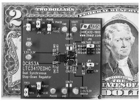
Figure 1. Dual buck regulator conserves space.
High Efficiency Dual Output
A typical application for the LTC3417 is shown in Figure 2. The two outputs of the LTC3417 are individually adjustable from 0.8V to 5V. VOUT1 can provide up to 1.4A of continuous current while VOUT2 can provide up to 800mA of continuous current, both at efficiencies of as high as 96%. OPTI-LOOP compensation allows the transient response to be optimized over a wide range of loads and output capacitors.
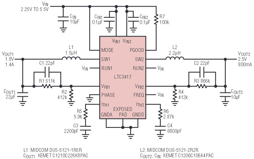
Figure 2. Dual output converter produces 1.8V at 1.4A and 2.5V at 800mA, with ceramic input and output capacitors.
Easy to Configure
The output voltages for the LTC3417 are set by the resistor dividers at the VFB pins, where the feedback voltage is compared to an internal 0.8V reference.
Major loop compensation adjustments are made with components at the ITH pins. The placement of the pole/zero combination is integral in the loop dynamics of the device, and consequently, different loop characteristics can be optimized with changes in these components, such as turn-on time, step response, and output ripple. Furthermore, the feed forward capacitor connected from VOUT to VFB also helps with step response and voltage ripple. In all, the designer using the LTC3417 has exceptional control over the loop characteristics.
Constant Frequency up to 4MHz for Noise Sensitive Applications
The LTC3417 uses a current mode, constant frequency architecture that benefits noise sensitive applications—the constant frequency of the oscillator simplifies noise filtering. The frequency of operation is set using the FREQ pin. When the FREQ pin is pulled high, to VIN, the internal oscillator runs at 1.5MHz. Pulling the FREQ pin low, through an external resistor, allows the user to vary the frequency anywhere between 600kHz all the way up to 4MHz. With a 143k resistor pulled from FREQ to ground, the frequency of operation is 1MHz.
High Efficiency at Light Loads
Efficiency at light loads is important in battery-powered applications since many portable applications spend most of their time in of standby or sleep mode. The LTC3417 offers three operating modes allowing the designer to optimize light load efficiency and noise: Burst Mode operation for the highest efficiency at light loads, pulse skipping mode for high efficiency and simplified noise suppression, and forced continuous mode for noise sensitive applications. The operating mode, for both outputs, is selected through the MODE pin.
Figure 3 shows the efficiency vs load current for all three modes for the 1.4A VOUT1 output. Figure 4 shows the efficiency vs load current for all three modes for the 800mA VOUT2 output. The external components used to take the data in Figures 3 and 4 are shown in the typical application schematic of Figure 2. In all modes, with no load, the dual converter draws only 100μA. In dropout, when the output voltage is within 100mV to 200mV of the input voltage, the internal P-channel MOSFET switch is turned on continuously, thereby maximizing the usable battery life. In shutdown, when both outputs are turned off (RUN1 and RUN2 are pulled to Ground), the LTC3417 draws less than 1μA, making it ideal for low current, long battery life, applications.
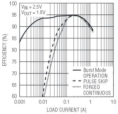
Figure 3. 1.4A VOUT1 Efficiency.
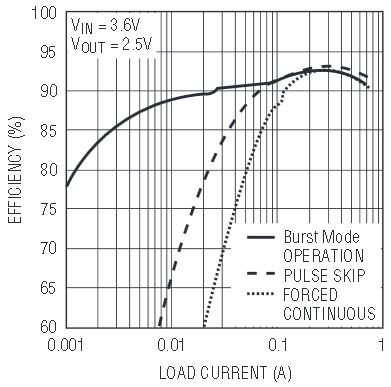
Figure 4. 800mA VOUT2 Efficiency.
Burst Mode operation achieves high efficiencies over a wide range of load currents. Burst Mode is selected for both outputs by pulling MODE to VIN. In this mode gate charge losses and internal quiescent current losses are minimized at low load currents thus achieving high efficiencies over a wide load current range. At low load currents, the control loop turns off all unnecessary circuitry, and stops switching for short periods of time. This generates variable frequency VOUT ripple components that change with load current. Of the three modes, the output voltage ripple is highest in Burst Mode operation—up to 25mVP–P.
Where supply noise suppression takes on more importance than efficiency, especially in telecommunications devices, pulse skipping mode can be selected by pulling the MODE pin to ground. This mode does not have the wide range of high efficiency that Burst Mode has, but the voltage ripple is minimized and the frequency components of that ripple are controlled over a wider load current range. At lower load currents, where the output skips pulses, there can be variable frequency components in the voltage ripple, but the ripple is only around 5mVP–P.
To reduce ripple noise even further use forced continuous mode. This mode decreases the ripple noise by sustaining the switching of the MOSFETS over all load currents, which results voltage ripple below 5mVP–P, while trading off efficiencies at low load currents. Since the MOSFETS are always switching, the voltage ripple is constant, allowing for better filtering of the voltage ripple noise. Forced continuous mode is selected by setting the MODE pin at VIN/2.
Out of Phase Operation Reduces Ripple and Increases Efficiency
To help reduce noise on the input voltage, and reduce the size of input capacitor, the two outputs on the LTC3417 can be selected to operate out of phase. The second output, when the PHASE pin is low, operates 180 degrees out of phase with the first channel. Out-of-phase operation produces lower RMS current on VIN and thus lowers RMS derating on the capacitor on VIN.
A High Efficiency 2.25V Dual Step-Down DC/DC Converter with all Ceramic Capacitors
The low cost and low ESR of ceramic capacitors make them a very attractive choice for use in switching regulators. Unfortunately, the ESR is so low that it can cause loop stability problems. Solid tantalum capacitor ESR generates a loop zero at 5kHz to 50kHz that is instrumental in giving acceptable loop phase margin. Ceramic capacitors remain capacitive to beyond 300kHz and usually resonate with their ESL before ESR becomes effective. Also, ceramic caps are prone to temperature effects, requiring the designer to check loop stability over the operating temperature range. For these reasons, great care must be taken when using only ceramic input and output capacitors. The LTC3417 helps solve loop stability problems with its OPTI-LOOP phase compensation adjustment, allowing the use of ceramic capacitors. For details, and a process for optimizing compensation components, see Linear Technology Application Note 76 (AN76).
Although the LTC3417 is capable of operating at 4MHz, the frequency in this application is set for 1.5MHz by connecting the FREQ pin to VIN.
Figures 5 through 7 show the trade off between mode and VOUT ripple noise. Figure 5 shows the voltage ripple at VOUT1 and the current through the inductor while the LTC3417 is in Burst Mode operation. The ripple voltage in this example was taken at an ILOAD of 40mA and is only 15mVP–P. The worst case output voltage ripple occurs just before the part switches from bursting to continuous mode, which occurs at about 250mA. At his point, the VOUT ripple can be as high as 25mVP–P.
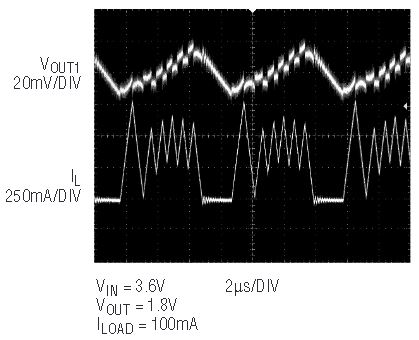
Figure 5. Burst Mode.
Figure 6 shows the VOUT1 ripple and the current through the inductor when the part is in Pulse Skipping Mode. Notice that the current through the inductor does go slightly negative, and then produces some high frequency components. The higher frequency components are due to the switching MOSFETS turning off. At lower currents, the part starts skipping pulses, and thus produces some lower frequency components. In this case, the voltage ripple does indeed show some higher frequency components, yet the ripple itself is at about 5mVP–P.
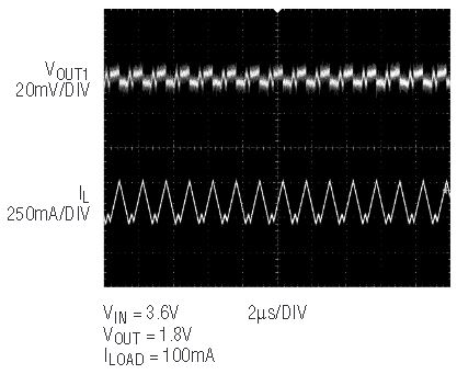
Figure 6. Pulse Skipping.
Figure 7 shows the voltage ripple at VOUT1 and the inductor current when the part is in Forced Continuous mode. Notice that the current through the inductor goes negative. At no time during Forced Continuous do the MOSFETS actually turn off, they keep switching. Therefore, the frequency component of the voltage ripple stays constant at the operating frequency. The voltage ripple therefore looks constant and stays below 5mV over all load currents.

Figure 7. Forced Continuous.
Conclusion
The LTC3417 is a dual synchronous, step-down, current mode, DC/DC converter designed to fit in the tight spaces afforded by today’s portable devices. Switching MOSFETS are integrated into the device, and high frequency operation enables the use of small sized components. It is also designed with versatility in mind with external components for loop compensation, variable frequency operation and different operating modes to optimize efficiency and noise.


