Differences Between the Ćuk Converter and the Inverting Charge Pump Converter
Differences Between the Ćuk Converter and the Inverting Charge Pump Converter
2016年03月07日
The Ćuk converter (also referred to as the two inductor inverting converter), the inverting charge pump and the single inductor inverting converter (also referred to as the inverting buck-boost) all provide a negative output voltage from a positive input voltage. However, engineers often unknowingly refer to these topologies by the wrong name, adding confusion to an area that already is a bit confusing. What does each topology do? Why choose one topology over the other? The reasons vary, with some being more obvious than others. The following discussion highlights differences between inverting power supply architectures, with an emphasis on intuitive thought rather than in-depth power supply design and switching theory. The objective is to show the advantages and trade-offs for the Cuk and inverting charge pump, followed by a brief discussion of the inverting topology, so you can make a more informed choice when selecting a negative output circuit topology that best suits your application.
The Ćuk Topology
The Ćuk topology can typically be obtained from a device that also provides a boost, SEPIC or flyback topology. The high voltage, low quiescent current LT8331 is an example of a device that can be configured as a Ćuk converter. It features a wide 4.5V to 100V input voltage range and includes a 140V, 0.5A power switch. Its 6µA quiescent current, programmable under voltage lockout, 100kHz to 500kHz switching frequency, and low output ripple make it ideal for high voltage, low standby current, negative output voltage needs.
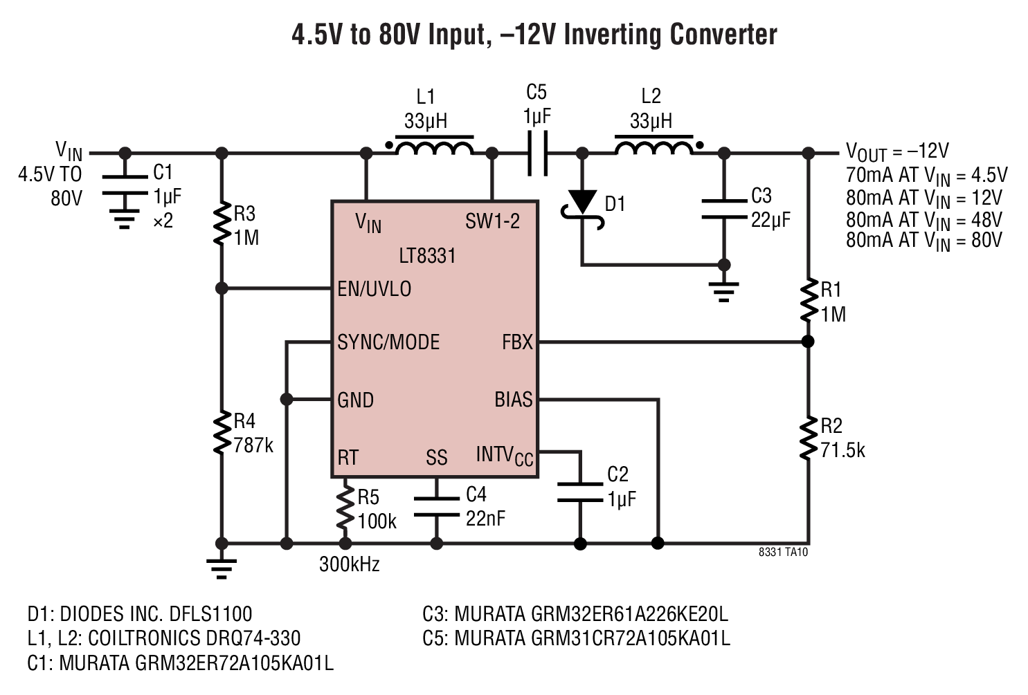
Figure 1. LT8331 Ćuk Configuration
It requires two inductors (these can be coupled or uncoupled and are typically matched in value) and a coupling capacitor (C5) between the input and output. The coupling or blocking capacitor receives energy from the input side of the circuit and transfers it to the output side of the circuit. With steady-state conditions (i.e. after power-up), the voltage across this capacitor is constant and approximately equal to VIN.
The Inverting Charge Pump Circuit
A variation of the Ćuk converter circuit is the inverting charge pump circuit where inductor L2 is replaced by Schottky diode D3 shown below. The LT3581 is a multitpology switching regulator with a 3.3A/42V power switch. It has built-in fault protection features to aid in protecting against output shorts, input/output overvoltages, and overtemperature conditions. Additionally, it includes a unique master/slave switch that makes it easy to build high voltage positive or negative voltages by stacking charge pump circuits.
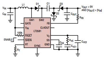
Figure 2. Inverting Charge Pump
The Ćuk vs. the Inverting Charge Pump
In figure 3 and figure 4, the Ćuk converter and the inverting charge pump converter topologies are shown side-by-side for comparison.

Figure 3. Ćuk Topology

Figure 4. Inverting Charge Pump Topology
Note that the two circuits look very similar; with the exception being the Cuk's second inductor has been replaced by a Schottky diode. Also, note they both have a lowside N-channel MOSFET (or NPN transistor) power switch. The lowside switch is also used in boost, SEPIC and flyback topologies, so these devices are quite versatile. The switch node always has a positive voltage applied to it. In a Cuk design, the feedback pin may or may not see a negative voltage (some devices do not allow negative voltages anywhere on the IC, some devices have a dual mode feedback pin that accepts both positive and negative voltages). Though similar in appearance, the operation of the two circuits is quite different.
The Ćuk Converter in More Detail
The Cuk can be used when the magnitude of VOUT is greater than or less than VIN. For the Cuk, the simplified duty cycle (assuming lossless diodes and switches) is given by:
Duty Cycle (D) = VOUT/(VOUT – VIN)
As VOUT becomes more negative, the duty cycle approaches 100% and as VOUT approaches zero, the duty cycle approaches 0%. The duty cycle is 50% when |VOUT| equals VIN.
Figure 5a shows the Ćuk current flow with the power switch closed and figure 5b show the Ćuk current flow with the power switch open.
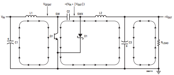
Figure 5a. Ćuk Current Flow with Power Switch Closed
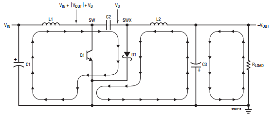
Figure 5b. Ćuk Current Flow with Power Switch Open
The current flowing from the input power source is continuous (in other words, current flows from the input when the power switch is closed or open). When the switch is closed, both inductors have an increasing current flow (the current is ramping up, but since the current in L2 is negative the two currents ramps move in opposite directions). The current in both inductors decreases when the switch opens. In figure 6 we see the average input current is simply the average inductor current ((ILAVG = Ipk + ILMIN)/2).
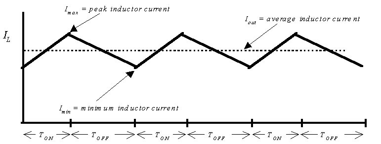
Figure 6. Ćuk Converter Input Current
Note the LC filters at the input and output of the circuit formed by the inductors and input/output capacitors. Continuous current flow combined with the LC filters results in a smoother input and output current, which in turn gives low output voltage ripple noise.
Keep in mind the optimal ripple current of the inductor should be about 40% of the output current. This is a good rule of thumb for most dc/dc converters and represents a trade-off between small inductor size and low switching losses.
For a Ćuk, this voltage is always positive. One cannot simply take a Ćuk converter and configure it as a single inductor inverter to reduce circuit components. Also, care must be taken to make sure the Ćuk power switch can handle the voltage VIN + |VOUT| appearing on the upstream side of the blocking capacitor.
The Inverting Charge Pump Circuit in More Detail
The inverting charge pump is closely related to a step-up converter because it combines an inductor-based step-up regulator with an inverting charge pump. Note in the figure 5a Ćuk circuit that the circuitry and current flow in the left most portion of the figure is identical to a boost converter. To this circuitry we add diodes and capacitors to obtain the inverting charge pump converter. Like the Ćuk, the inverting charge pump has continuous input current, but unlike the Ćuk it has discontinuous output current. This configuration often provides the best combination of size, efficiency and output ripple for a given output current. The inverting charge pump topology can only be used when the magenitude of VOUT is greater than VIN. For cases where the magnitude of VOUT is less than or equal to VIN, use a different topology such as a Ćuk, inverting converter or an inverting flyback.
Though it uses a charge pump, fairly high load currents can be obtained because the inductor is the main energy storage element rather than a flying capacitor. Figure 7 below shows the LT3581used as an inverting charge pump (upper circuit) and a boost converter.
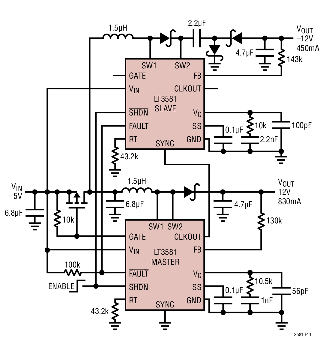
Figure 7. LT3581 Inverting Charge Pump Plus Boost
The LT3581 has master/slave switches instead of a single power switch, and Schottky diode between pins SW1 and SW2 is used to isolate the switches so the current spike through coupling capacitor C1 (created when the power switch turns on) flows only through the slave switch and not the master switch (where the current comparator resides), thereby preventing the internal current comparator from falsely tripping. When the power switch turns off, the voltage at the switch node flies back to VIN + |VOUT| as energy is transferred to the output capacitor and load. Output disconnect is inherently built into this single inductor topology.
For the inverting charge pump, the simplified duty cycle is given by:
Duty Cycle (D) = 1 – (VIN/|VOUT|)
Since |VOUT| is always greater than VIN, the duty cycle is near 0% when they are equal and increases as VOUT becomes more negative.
In the inverting charge pump configuration below, a resistor is added in series with the Schottky diode between the negative output and the D pin of the LT3483/LT3483A. The purpose of this resistor is to smooth/reduce the current spike in the capacitor C2 when the switch turns on. A 10Ω resistor works well in this application (Li+ battery to –22V@8mA), and the impact to converter efficiency is less than 3%. The resistor values recommended in the applications circuit also limit the switch current during a short-circuit condition at the output.
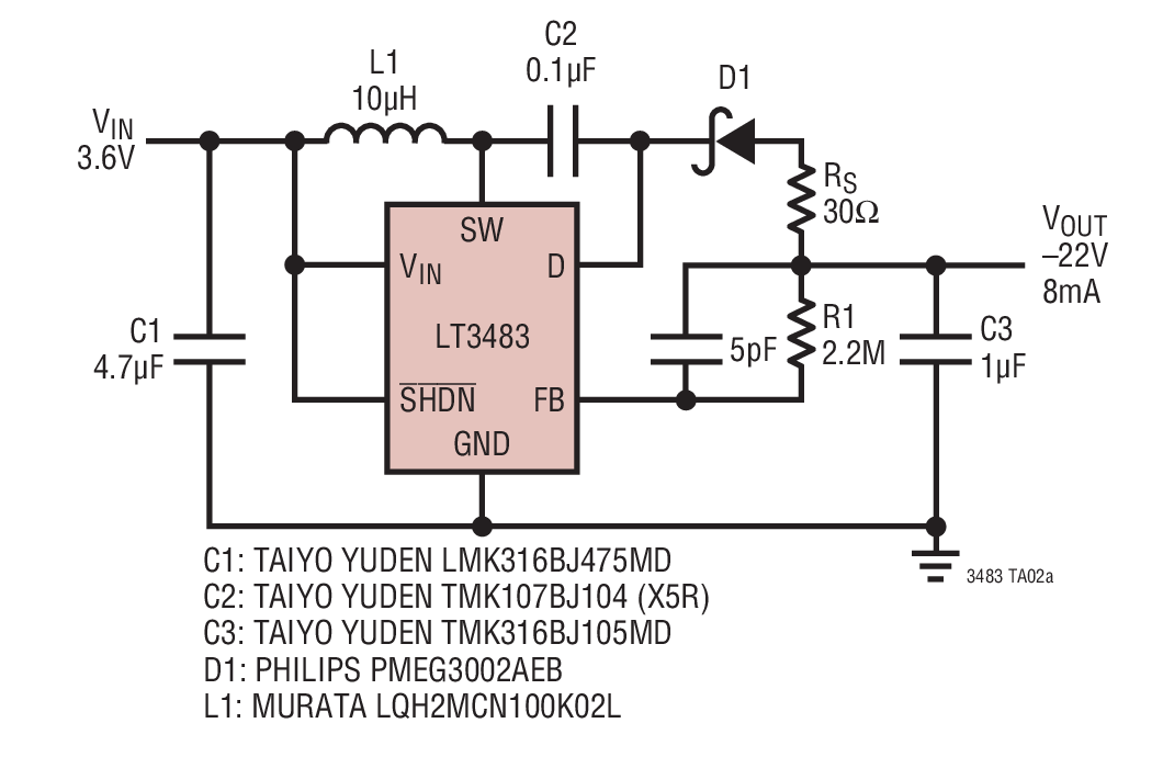
Figure 8. LT3483 Circuit with Added Rs Resistor
The Inverting Topology
The inverting topology uses a single inductor and does not require a coupling capacitor; thus it requires fewer components as shown below. An example of the single inductor inverting topology is shown in figure 9 below using the LTC3863 inverting controller with external power switch. The LTC3863 has a 3.5V to 60V input voltage range, a low 70µA quiescent current, and it allows output voltages below –150V. Since the power switch must see a negative voltage, the inverting topology is less versatile in that it can only be used for negative voltages. It also has higher peak current and output ripple than a Cuk converter with a similar output current. For the LTC3863, the external power switch allows the user to choose the best MOSFET for the peak current and output voltage desired.
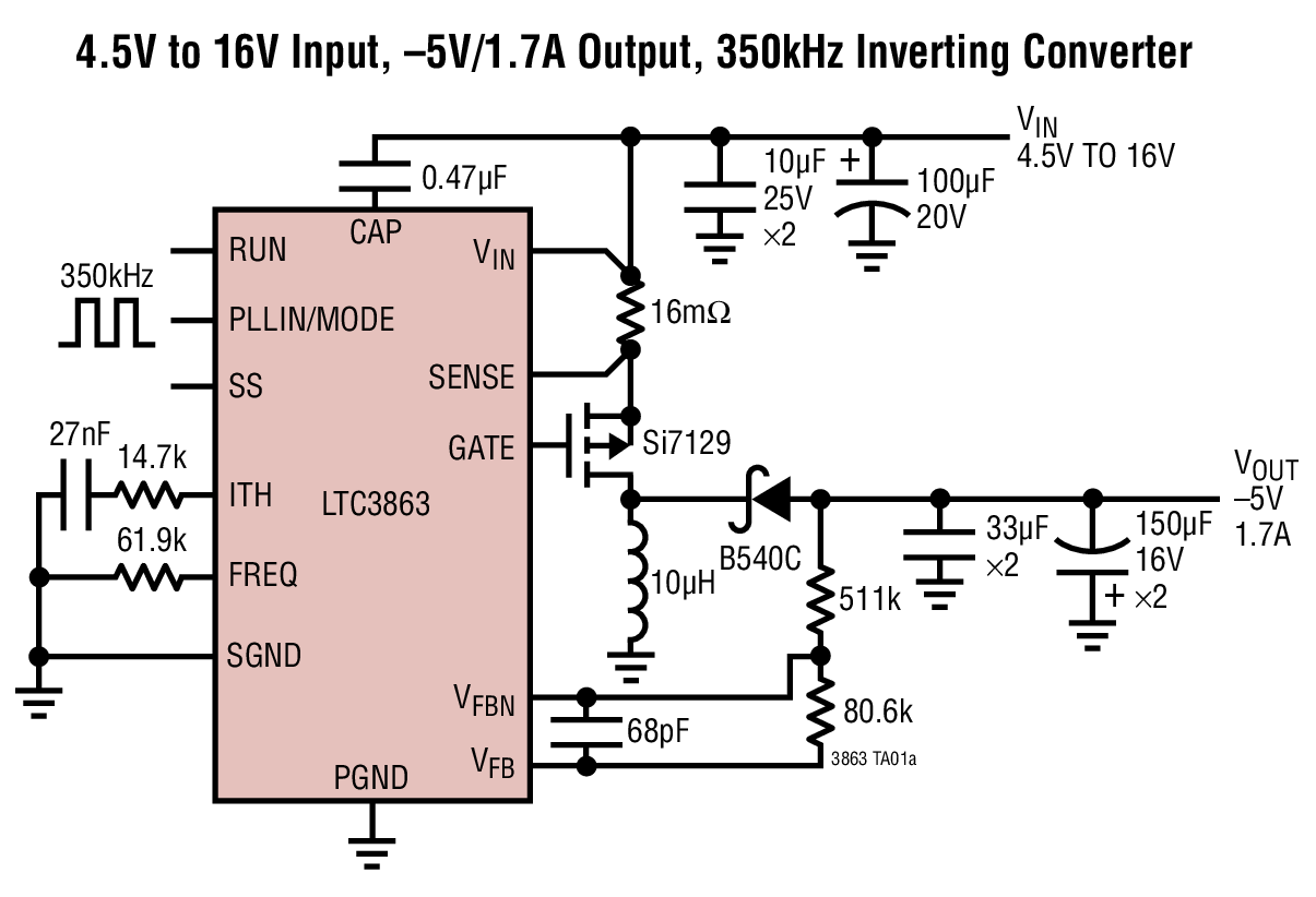
Figure 9. LTC3863 Inverting Converter
The duty cycle for the inverting topology is the same as that of the Cuk converter, namely
Duty Cycle (D) = VOUT/(VOUT – VIN)
Similarly, given the same output voltage, input voltage and switching frequency, the circuits have the same duty cycle and the same inductor current slope (namely the ripple current, which equals VIN*tON/L). Let's look at the current flow during switching cycles for each topology.
Figures 10a and 10b show the current flow with the power switch closed and open.
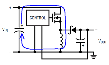
Figure 10a. Inverting Circuit Current - Switch Closed
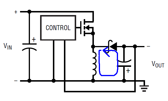
Figure 10b. Inverting Circuit Current - Switch Open
For the inverting converter, current flows from the input power source only when the switch is closed. This results in a pulsed input current rather than continuous current flow.

Figure 11. Inverting Converter Input Current
Unlike the Ćuk, the inverting circuit's average input and peak current are a function of duty cycle. At 50% duty cycle, the average input current is roughly two times that of the Ćuk (assuming no other circuit losses). Since we are dealing with power transfer, as the output voltage becomes more negative or the input voltage decreases, the peak inductor current increases, increasing output ripple noise; similarly, as the input voltage increases or the output voltage approaches 0V, the peak inductor current decreases. In both cases, the inductor current can be continuous and the input current can approach being continuous, but it never is continuous. So it makes sense that for a given output current, the Ćuk converter has a lower peak input current (and output current since the two inductor currents are similar) and lower output voltage ripple noise than an inverting converter topology.
Another difference between the topologies is the voltage at the switch node. For the inverting converter, this voltage is negative during the 2nd phase of the switch cycle. Therefore the topologies are not readily convertible from one to the other.
In Summary
The Ćuk, inverting charge pump and inverting topologies provide a negative output, but each configuration has nuances that can provide a benefit when designing a negative power supply. In addition to these circuits, the buck converter with the output referenced to ground, and the flyback converter are also capable of providing a negative output voltage. Unfortunately, many data sheets and online search parametric tables do not distinguish between the unique topologies, but rather lump them together as "inverting converters." However armed with knowledge about the differences, you now can make a wiser choice when the time comes for you to select an IC for your system power.
著者について
Kevin Scottは、アナログ・デバイセズのパワー製品グループでプロダクト・マーケティング・マネージャを務めています。昇圧、昇降圧、絶縁型コンバータに加え、LEDドライバとリニア・レギュレータを担当しています。以前は、シニア・ストラテジック・マーケティング・エンジニアとして、技術トレーニング用コンテンツの作成、セールス・エンジニアのトレーニング、各種製品の技術的な優位性を紹介するウェブサイト向け記事の執筆を行っていました。半導体業界で2...
Jesus Rosalesは、アナログ・デバイセズのアプリケーション・グループ(カリフォルニア州ミルピタス)に所属するアプリケーション・エンジニアです。1995年にアソシエート・エンジニアとしてLinear Technology(現アナログ・デバイセズ)に入社し、2001年にアプリケーション・エンジニアに昇格しました。それ以来、モノリシック型の昇圧/SEPIC/反転コンバータ・ファミリと、オフライン型/絶縁型アプリケーション・コントローラを...


