A Composite Amplifier Topology Wrings More Performance Out of the LTC1597 16-Bit Current Output DAC
A Composite Amplifier Topology Wrings More Performance Out of the LTC1597 16-Bit Current Output DAC
2002年03月01日
The LTC1597 16-bit current output DAC is capable of settling in the neighborhood of 1.7µs to 2µs using the 16-bit accurate LT1468 as an I-V converter1. For applications needing higher throughput such as in-circuit testing, electrostatic sorting of organic materials, or electrostatic actuation of MEMS as examples, 1µs settling seems to be a common goal. This article shows a composite amplifier that can achieve settling in 1µs.
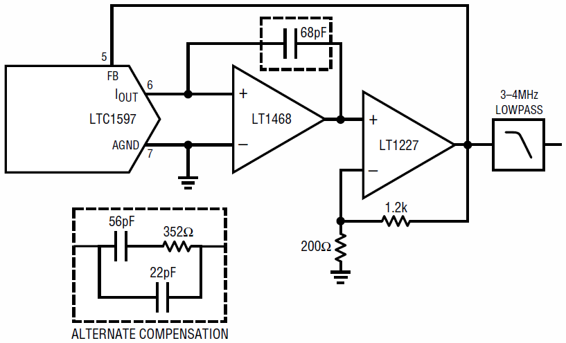
The topology shown in Figure 1 combines the low noise, low offset, low input current qualities of the LT1468, with the fast slewing output of the LT1227. The output of the first stage is still taken as the node that drives the compensation capacitor, but the second stage, the LT1227, configured with a closed loop gain of +7 produces the output, and is the source for global and DC feedback.

Figure 1. Fast settling current output DAC.
However, as there is no bandwidth limiting in the second stage other than the amplifier itself, the wideband noise of the amplifier produces considerably more than 1 LSB of noise.
In addition, there is peaking in the first stage due to the effect of the large capacitance at the output of the DAC. The noise from the first amplifier is also amplified by the fixed gain of the second. This then requires bandwidth limiting to bring the noise level down to a level that could be considered acceptable using the common expectation that the signal remain within 1 LSB after settling. A 1st order 2MHz lowpass as shown will extend the settling time on the order of 5%. Note that settling time is DAC input code dependent.
A factor of two improvement in settling time would in itself be considered worthwhile, but perhaps more importantly for many applications of this part, it gets close to the target output considerably faster, and in a more consistent fashion across code changes, and amplitudes. In addition, as the composite does not spend as much time in a slew rate limited state, harmonic distortion is reduced.
The topology with the LT1468 by itself will be slew rate limited for any significant code changes. In the case of waveform generation, the slew rate limiting in itself is responsible for odd order harmonic distortion, and inter-modulation distortion. Any mismatch between positive and negative slewing, is responsible for 2nd harmonic distortion.
If the LTC1597 is used for waveform generation below a few kHz, these effects are not very significant, and 2nd harmonic distortion is on the order of –95dB, but above 5kHz to 10kHz, the slew limit related distortion becomes increasingly significant. At 20kHz, the slew rate of the LT1468 will limit a full-scale signal to a spurious-free-dynamic-range figure (SFDR) of about 70dB. At 20kHz, the composite produces on the order of –95dB SFDR. Similar improvement in multiplying applications can be achieved.
You will notice that the compensation capacitor is larger in the case of the composite, and yet the combination is faster. A larger cap is required because the signal swing at the output of the LT1468 is reduced by the same factor as the close loop gain in the output stage. The phase margin in the case of the composite is improved by virtue of the phase shift associated with the pole in the DAC feedback path being reduced to a greater extent due to the greater relative value of the compensation capacitor.
As there is more phase margin, as well as about 16dB more open loop gain, the variability of settling times versus code is reduced. Variability in settling time is due to variation in feedback factor, or noise gain, in the I-V stage, as well as variation in phase margin with changes in output capacitance and noise gain. Feedback factor is normally 2 in the case of an amplifier configured for an inverting gain of 1. Compensation is normally a compromise between overcompensation at one extreme of noise gain, and under compensation at the other. Note that noise gain at higher frequencies is influenced by the DAC output capacitance and the compensation capacitor.
In the case of the single amplifier IV stage, the use of a larger than optimal compensation capacitor, while improving the phase margin, results in attenuation of the higher frequency components of the transient, hence the settling is slowed, or overcompensated. If there is inadequate compensation capacitance, there is not enough phase margin as a result of the pole in the feedback network, and the amplifier will ring, possibly indefinitely.
Note that the stability of this composite is dependent on a dominant pole in the first stage, and a second stage that is much faster, in order to maintain adequate phase margin around the entire loop. Resist temptation to put a capacitor in the feedback loop of the LT1227, and do not substitute with an appreciably slower amplifier.
If you need low noise at the output of this DAC, the bandwidth reducing filter must follow the output.
The degree to which settling is extended is determined by the nature of the filter used, but a lower order filter is likely to be better in most cases, as it serves the purpose of reducing noise bandwidth, but is less likely to ring. A noise bandwidth of 3–4 MHz will reduce noise to the 1 LSB level. A degree of under-compensation will compensate for the effect of the filter, and allow settling times that are very similar to optimal compensation without the filter.
For situations where getting close fast is important, the output of this composite will get to within 12-bit accuracy within about 200ns versus approximately 1µs for the LT1468 alone.
There are some other subtle performance benefits of this composite. The LT1468 is not obliged to drive any significant output current in driving only the LT1227 input, and hence will not exhibit any thermal tails. The settling time of these circuits is variable due to variation in DAC feedback resistance, and output capacitance, as well as variation in LT1468 slew rate. If optimal results are required in either the original topology or the composite, trimming may be required.
The LT1468 alone is a simpler and lower power solution than the composite and depending on noise requirements, may not require an output filter. In the event that the load cannot be driven via the higher output impedance of the filter, the original topology may be a better choice. If the original is not fast enough, or if lower harmonic distortion is required, try the composite.
Figure 1 includes an alternate compensation scheme, which compensates for the output de-glitcher switch impedance built into the LTC1597.
1 For more about the high speed settling performance of the LTC1597, used in conjunction with the LT1468, and how to measure it, see Application Note 74 by Jim Williams.
著者について
この記事に関して
製品
製造中
140MHzビデオ帯域電流帰還型アンプ
製造中
90MHz、22V/μs、16ビット精度オペアンプ
製造中
14ビットおよび16ビット・パラレル、低グリッチ乗算型DAC、4象限抵抗付き


