Combo Hot Swap/Load Share Controller Allows the Use of Standard Power Modules in Redundant Power Systems
Combo Hot Swap/Load Share Controller Allows the Use of Standard Power Modules in Redundant Power Systems
2003年01月01日
Introduction
High power, high-reliability electronics systems depend on power supply load sharing to handle the heavy current loads and to increase system robustness. Usually the load is shared between modular DC/DC converters operated in parallel, a topology that offers several advantages depending on how it is implemented:
- Redundancy. Typically, load sharing power supplies can provide more power than the system can use. This way if any of the power supplies fail, the remaining power supplies can still support the load. Redundancy requires that a failed power supply is automatically isolated from the system, and that it can be replaced without interrupting the system power.
- Reliability. The reliability of the system depends in large part on the current sharing capability of the power supply modules. Ideally, the current is distributed evenly amongst the power supplies, so that on average each module dissipates equal heat. This in turn increases system lifetime.
- Efficiency. For very high power systems, significant efficiency gains can be achieved by operating converters at their most efficient operating point, which is somewhere in the middle of a converter’s operational load range. In a parallel multi-converter architecture, efficiency is clearly at maximum when each converter operates at this optimum point. The only way to achieve this over a wide load range is to enable or disable converter modules as load requirements change, in order to keep the enabled modules operating at loads near their maximum efficiency. The LTC4350 makes this possible via its Hot Swap™ feature, which allows modules to be disabled or enabled on the fly without interrupting the power bus.
The LTC4350 simplifies the design of load sharing systems by combining both a load share controller and a Hot Swap controller in one package. The load share controller equalizes the current handling of each parallelled power supply, and the Hot Swap controller allows power supply modules to be safely removed from, or inserted into, a hot system.
Overview of the LTC4350’s Features
The LTC4350’s load share and Hot Swap controllers are connected by internal logic which coordinates load-sharing and hot swapping activities. The LTC4350’s load share controller is a closed loop control system with a full set of features including precise voltage control and accurate current sharing. The closed loop control system has defined bandwidth and transient characteristics.
The LTC4350 protects the system it is powering from overvoltage and undervoltage conditions with separate overvoltage (OV) and undervoltage (UV) comparators, each with its own reference source. A timer sets the delay between events, when the UV pin goes high, and when load sharing turns on.
The LTC4350 enables active current sharing between the power supplies using an inner current loop and an automatic master outer voltage loop controller assignment. The power system based on the LTC4350 controllers with n power channels is shown in Figure 1. Each channel consists of the power module (DC/DC Converter); one LTC4350; a bidirectional power switch which connects the power module output to the load (a series connection of the two MOSFETs Q1 and Q2); a current sense resistor RSENSE; a few passive components to set loop compensation; and miscellaneous feedback circuitry. Each power module is controlled by one LTC4350. The LTC4350 SB (share bus) pins are connected together to form the load share bus. The voltage drop on the sense resistor RSENSE is used as a feedback signal in the current control loop. The output voltage of each module is modified by the LTC4350 so that each module contributes an equal amount of current to the load.
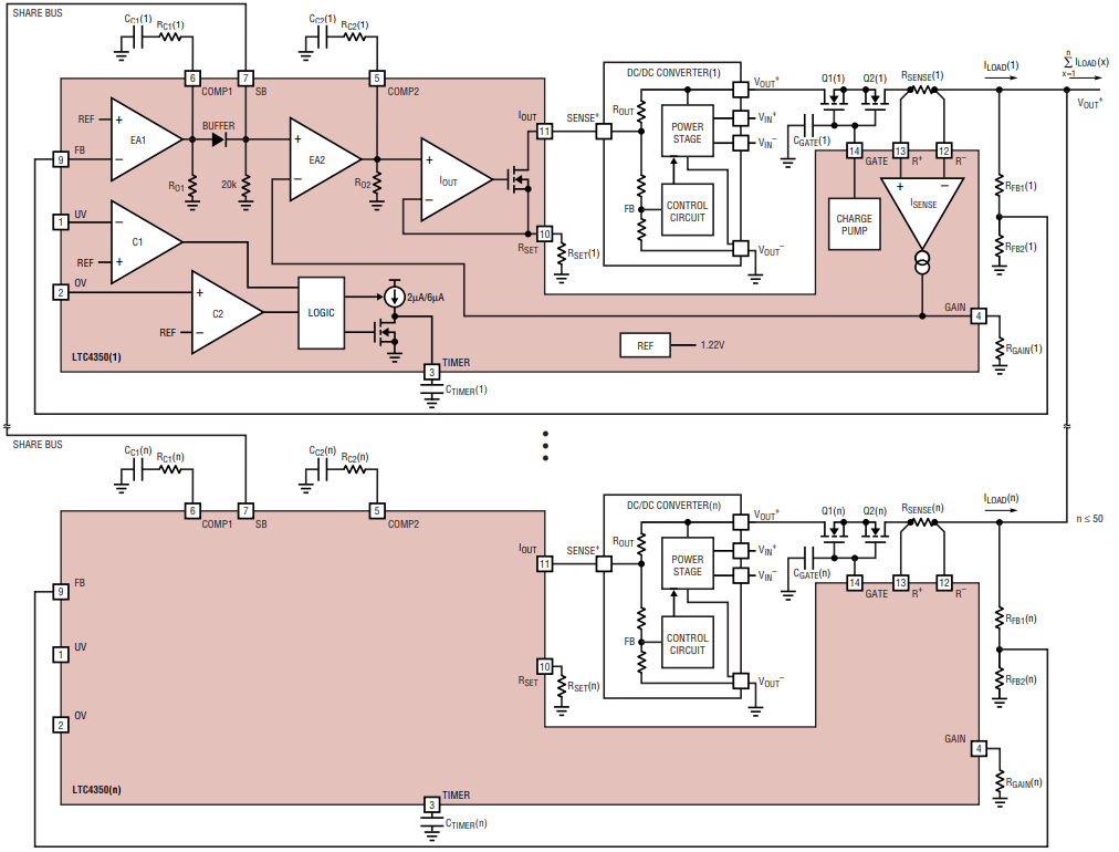
Figure 1. LTC4350-based power system.
The LTC4350 uses the power module remote sense input to adjust the power module output voltage. Each power channel is a 2-loop control system, the inner loop is a current control loop and the outer loop is a voltage control loop. The share bus voltage serves as the common command signal from the outer voltage control loop to all the current control loops, for each power module.
The current control loop includes:
- the current loop error amplifier (EA2) which includes compensation network RC2CC2;
- the voltage-to-current converter to drive the module’s sense resistor (ROUT);
- the DC/DC converter module (as the plant of the loop);
- a load current sense amplifier consisting of current sense resistor RSENSE and current signal amplifier ISENSE (which uses a resistor connected to ground from the RGAIN pin to set the current to voltage transfer ratio).
The voltage control loop includes:
- the voltage error amplifier (EA1) which includes compensation network RC1CC1;
- the internal 1.220V reference;
- the previously mentioned closed current loop;
- feedback divider (RFB1RFB2).
Only one voltage control loop is active, the other controller voltage error amplifier outputs are isolated by series diodes between the amplifier outputs and the share bus. This automatic selection of a master voltage control loop is the result of component tolerances. The voltage error amplifier providing the highest output level reverse biases the series diodes of all the other error amplifiers. If the channel functioning as the master controller fails or is removed from the system, the controller with the next highest output level becomes the master.
The LTC4350’s hot swapping feature eliminates power supply transient stress in hot-insertion and hot-removal and isolates faulty modules by disabling the external power switch. The failed supply can be removed and replaced with a new one without interruption to the power system. The hot swap circuitry consists of the gate driver (pin 14) and the reverse current comparator.
Figure 1 shows a system with n power supplies and n LTC4350s, where n ≤ 50. Each power channel is connected to the system power bus identically by paralleling the share bus (SB), positive (OUT+) and negative (OUT- or GND) outputs.
The LTC4350 is packaged in a 16-pin IC narrow SSOP package and operates over the range of 1.5V to 12V, which can be extended down to 1V with auxiliary circuitry. It should be noted that the share bus maximum voltage and gate voltage are a function of the LTC4350 supply voltage (VCC).
Hot Swap FET Gate Drive Characteristics
The Hot Swap FET switch gate turn on voltage slew rate is a function of total gate capacitance including any additionally added capacitance and the 10µA charge pump output current as given by:

where CGATE is in µF
The 10mA high current sink capability of the gate pin shuts the FET switch off almost 1000 times faster than FET turn on.
Tailoring the Control System to Various Power System Designs
The wide range of available power modules, each with a different dynamic characteristics, requires tailoring the current and voltage control loops for each power system design.
The voltage loop and current loop error amplifiers EA1 and EA2 are transconductance amplifiers with output impedances of RO1 and RO2 and transconductances of gm1 and gm2. The use of transconductance error amplifiers provides a simple means of compensation using simple RC shunt networks to ground.
Adding a shunt capacitor to ground converts the transconductance amplifier into a dynamic block with the transfer function of:

where GEA = gmRO and TP = CCRO
which includes the effect of the finite output resistance RO.
The insertion of a resistor in series with the shunt capacitor adds a zero to the transfer function:

where:
2πfp = ωp = 1/Tp = 1/CC(RO + RC) is the pole frequency,
GEA = gmRO is the error amplifier gain,
RC and CC are compensation components,
and TZ = Main time constant of the power converter.
The error amplifier parameters are not specified in the data sheet, but typical values are shown in Table 1.
| Parameter | EA1 Voltage Error Amp | EA2 Current Error Amp |
| RO | 24.7 × 10⁶Ω | 8.5 × 10⁶Ω |
| gm |
0.769kΩ–1 | 0.25kΩ–1 |
A power channel control system block diagram for dynamic analysis is shown in Figure 2.
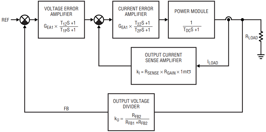
Figure 2. Power channel control system block diagram.
Operating Modes and Design Considerations
Load Share Controller Operation
LTC4350 performs load sharing as follows. All power supplies are preliminarily adjusted to 250mV–300mV below the desired output voltage. Each LTC4350 can increase the output voltage of its respective power module by creating an additional voltage drop across ROUT—that is, the IOUT amplifier sinks current through ROUT to increase the module’s output voltage. The LTC4350, using feedback from the common load share bus and the inner current loop, adjusts each supply to the desired output voltage and balances the load across all the supplies.
The LTC4350 can control output voltages down to 1.5V without the use of auxiliary circuitry. (To use the LTC4350 with output voltages below 1.5V, see Figure 6.) The LTC4350 has an internal 1.22V reference. The voltage feedback divider resistors for the outer voltage control loop are calculated from:
VOUT = VREF(1 + RFB1/RFB2)
where VREF = 1.22V
Hot Swap Controller Operation
The LTC4350-controlled external power switch allows power supplies to be hot swapped in and out of the powered system, minimizing disturbances on the system power bus. The external capacitance at the GATE pin is charged and discharged by constant current sources and controls the rate of turn on and turn off of the external FET switch. The undervoltage and overvoltage comparators in the LTC4350 monitor the power module and only enable the hot swap function when the power module output voltage is within tolerance. When the power supply is disconnected, the undervoltage comparator indicates a fault condition, the power switch gate is quickly discharged and the load is isolated from the power supply.
Special attention should be paid to choosing the gate voltage slew rate. The gate voltage slew rate should be chosen such that the load share control loop can prevent excessive reverse current flow into the power supply output capacitors when the external FET switch closes and load share is activated. The LTC4350 monitors reverse (negative) current flow. The reverse current limit (RCL) set point is calculated from:
IRCL = 30mV/RSENSE
One way to minimize the amount of reverse current is to minimize the bulk capacitance on the power module side of the MOSFET—taking the minimum capacitive loading requirements for the power supply module into account. If the DC/DC converter is capable of converting energy in both directions (source or sink current) the high reverse current in the transient caused by powering up additional modules can reach the reverse current protection level IRCL. The only solutions are to reduce the external MOSFET gate slew rate and/or set the IRCL threshold higher by lowering RSENSE. Both solutions add their own problems, though. Reducing the MOSFET slew rate slows the disconnect rate of a failing or faulty power module (the two rates are directly proportional, both based on the GATE pin capacitance). Reducing RSENSE lowers overall gain. A balance must be struck with these competing requirements.
Protection Features
The LTC4350 can identify faults in the power supply and isolate it from the load when an external MOSFET power switch is used. In the case of a power supply output short to ground, the reverse current detector senses that the voltage across the current sense resistor has changed direction and has exceeded 30mV for more than 5µs. The power switch gate is immediately pulled low disconnecting the short from the load. The external MOSFET gate is allowed to ramp-up and turn-on the power switch as soon as the reverse voltage across the sense resistor is less than 30mV and the module output voltage is within the undervoltage–overvoltage comparator window. The condition where a power supply output shorts to high voltage is detected as an overvoltage fault. In this case, the gate of the power switch is pulled low, disconnecting the overvoltage from the load.
The STATUS pin state reports any of three types of faults. The first is undervoltage lockout when the UV pin falls below 1.220V while the output voltage is active. The second failure is an overvoltage condition when the OV pin is above 1.220V. The third fault is an overload or open supply output condition when the COMP2 pin is above 1.5V or below 0.5V and the voltage on the GAIN pin is greater than 100mV.
Control System Compensation
The design approach for the control system loop is to maximize the power system bandwidth. Besides the obvious benefits of the fast system and transient response, a high control loop bandwidth minimizes disturbances when connecting the power supply output to the operating bus.
The optimum solution for a power channel with a DC/DC converter and an LTC4350 load share controller is to design the load share inner current control loop channel bandwidth equal to, or close to, the DC/DC converter bandwidth, and the voltage loop bandwidth 5% to 10% higher than the current loop bandwidth.
It is important that the step response of the closed current loop should be similar to the response of a first order system or second order system with a damping ratio of ζ ≥ 0.75. If this condition is not met, the step response will not be monotonic and will result in chattering oscillation as the voltage control loop keeps changing masters and the module output currents oscillate about their equilibrium values.
The control loop design starts with characterizing the DC/DC converter response. If the converter behaves like a first order system, the converter loop time constant, TDC, can be calculated from the converter’s 3dB frequency response, ωCROSS, by ωCROSS = 1/TDC.
To realize the maximum current loop bandwidth, which is equal to the DC/DC crossover frequency ωCROSS, a current loop compensation network of the form:

is required where T2p and T2z, are the pole and zero time constants of the current loop error amplifier EA2. The maximum stable bandwidth is obtained when T2z = TDC. With any larger T2z, the current loop bandwidth, ωCURRENT, will be less than ωCROSS. The current error amplifier EA2 pole T2p is used to set the overall open loop gain and must take into consideration the other gain terms in the current loop transfer function such as the load current sense amp ISENSE and the voltage-to-current converter IOUT. The requirements for setting the gains of these other blocks are discussed later. Figure 3 shows the response of a current control loop meeting the above criteria for 1st order plant compensation.
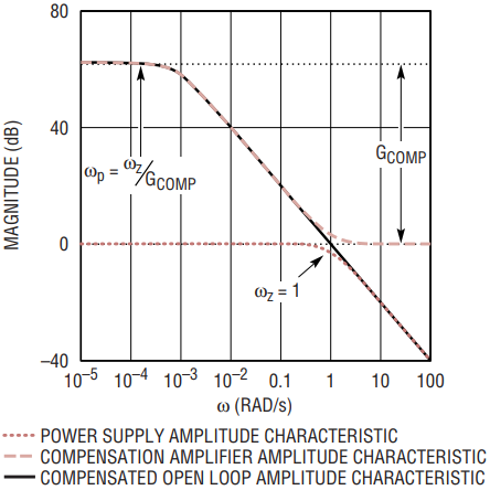
Figure 3. 1st order plant compensation.
If the converter behaves like a second order system, the crossover frequency of the inner current control loop is reduced so that the composite loop behaves like a first order loop or an overdamped second order loop with ζ ≥ 0.75. This is achieved by matching the control loop zero T2z to the cross over frequency of the power module. T2z = 1/ωCROSS and then suppressing the gain of the control loop by 10dB to 15dB by adjusting T2p appropriately. Figure 4 shows the approach to 2nd order power module compensation.
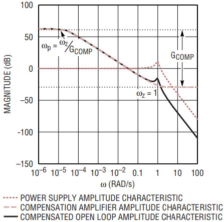
Figure 4. 2nd order plant compensation.
The other elements in the LTC4350 current and voltage loops must be chosen so as to guarantee normal loop operation up to the actual current limit, IL, of the power module regardless of how much IL exceeds the modules maximum output current specification. The maximum feedback current signal (voltage on the GAIN pin) must be lower than the maximum share bus voltage (VSHARE BUS (MAX)) at an output current of IL, where VSHARE BUS (MAX) is the lesser of [(VCC – 1.5V) and (5.6V)].
This requirement has implications on the selection of RSENSE and RGAIN:
ILRSENSERGAIN/1kΩ ≤ VSHARE BUS (MAX)
RSENSE is chosen to provide the necessary 30mV reverse current detection at an acceptable fault current limit while minimizing power loss and forward voltage drop. The value of RGAIN is then derived using the previous equations above maximizing the output voltage within the constraints of VSHARE BUS (MAX).
The current control loop error amplifier output voltage level of EA2 is converted to a current (by the IOUT block), which is used to modulate the power module output voltage. The maximum output current capability of IOUT is 20mA. The LTC4350 current measurement system gain is set by resistor RSET connected between ground and the RSET pin. The current range should be selected such that the LTC4350 can realize a 1V control range on the power module. This current is drawn from the +SENSE terminal of the power module. If the internal-resistance ROUT between +VOUT and +SENSE is less than 50Ω, an external driver is needed to boost the 20mA maximum current to achieve the required 1V control range. The design example in figure 5 shows a circuit to boost the IOUT current.
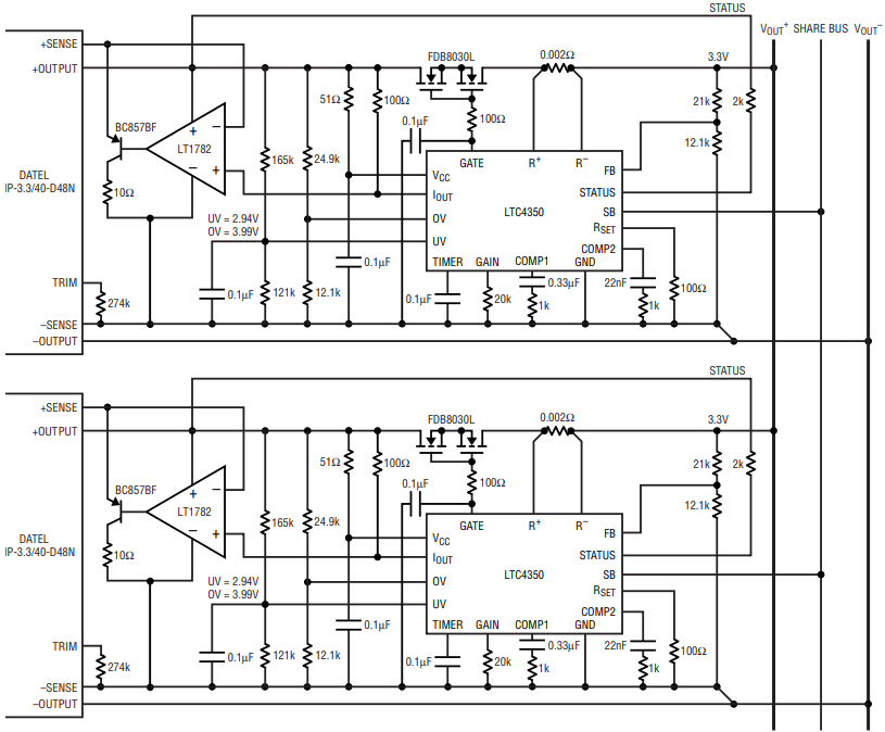
Figure 5. 3.3V Load share controller for DATEL® power modules.
The open loop transfer function for the inner current control loop is:

T2p is calculated by setting |LT| = 1 at ωCROSS for a first order loop and for a 2nd order underdamped loop, T2p is increased by a factor of 3 to 5 so that the loop crossover occurs below the peak in the module frequency response.
The overall voltage loop crossover frequency at ωVOLTAGE should be set 5% to 10% above the current loop crossover frequency ωCROSS. This prevents interaction between the inner current and outer voltage loops such that the output voltage responds quickly to transients and then the current control loop adjusts each power supply so that the loads are balanced.
Design Examples
A dual supply load share design example is shown in Figure 5. This design uses DATEL power modules with an ROUT < 50Ω. To provide the required voltage control range, the IOUT current is boosted with an external current amplifier.
To load share power supplies with output voltages below 1.5V, the feedback voltage must be amplified to match the 1.22V internal reference on the feedback pin as shown in Figure 6.
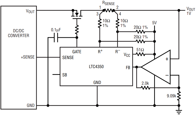
Figure 6. Example of 1V load share implementation (one channel).
Conclusion
The LTC4350 combines Hot Swap and load share functions into one IC, making it possible to provide effective power management solutions using standard off the shelf DC/DC converter modules. The LTC4350 also simplifies the design of custom supplies. The Hot Swap and load share functions work in concert to facilitate the addition of power system features that improve overall reliability and reduce down time, including fault isolation and identification, Hot Swap replacement of failed modules, redundancy, and improved thermal management.


