CMOS Switches Offer High Performance in Low Power, Wideband Applications
CMOS Switches Offer High Performance in Low Power, Wideband Applications
2004年02月01日
The performance of CMOS switches has increased to the point that they have broken the 1-GHz barrier, and are now able to compete with GaAs switches.
High performance RF switches are among the key building blocks required in modern wireless communication systems. Switches that provide low insertion loss, high isolation between ports, low distortion and low current consumption are much sought after for high frequency applications such as phase shifters, switchable filters, transmitters and receivers for radar systems—ranging from large installations to anti-collision radar in cars—and communication systems from base stations to cell phones.
Traditionally, only a few processes were available for developing good wideband/RF switches. Gallium arsenide (GaAs) FETs, PIN diodes and electromechanical relays have dominated the market, but standard CMOS is now making its mark.
GaAs has been popular because of its low on resistance, low off capacitance and high linearity at high frequencies. As CMOS process geometries continue to shrink, the performance of CMOS switches has increased to the point that they have broken the 1 GHz barrier, and are now able to compete with GaAs switches. Designed to maximize bandwidth while maintaining low cost, CMOS switches offer an alternative to expensive GaAs switches in low cost, low power applications.
This article explains the key specifications associated with wideband switches, traditional methods used for wideband switching, and the benefits of CMOS switch technology. It also shows how new CMOS switches can outperform GaAs switches in low power, high frequency applications. This should convince you that CMOS wideband switches are ideal solutions for applications such as cable modems, MRI scanners, xDSL modems, next-generation cordless phones, and applications in the aviation industry that require an operating frequency up to 1 GHz and beyond.
Wideband Switch Basics
Wideband switches are designed to meet the demands of devices transmitting at frequencies up to 1 GHz and higher. The selection of devices for these types of applications is completely dependent on how they perform over frequency. There are two important ways to describe the performance of an RF switch: the insertion loss in the closed state and the isolation in the open state.
Insertion loss is the attenuation between input and output ports of the switch when the switch is on. Low insertion loss is critical for systems that require a low overall noise figure. Because the switch is one of the first components in the signal path, the minimum receivable signal is very important. Figure 1 shows a typical plot of insertion loss versus frequency for the ADG919.
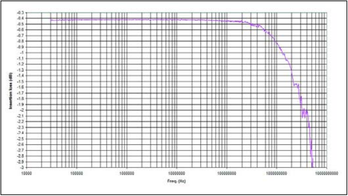
Figure 1. Insertion loss vs. frequency for the ADG919.
This plot shows that the insertion loss is less than 0.5 dB out to 100 MHz, 0.8 dB at 1 GHz, and 1.5 dB at 2 GHz. This is comparable to many GaAs switches with typical values between 0.7 dB to 1 dB at 1 GHz.
Off isolation is defined as the attenuation between input and output ports of the switch when the switch is off. Figure 2 shows a typical plot of off isolation versus frequency. High isolation is demanded for most wideband switching, and is generally a critical specification in determining if a part is suitable for a particular application.
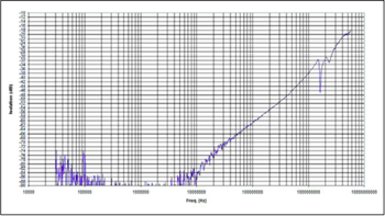
Figure 2. Off isolation vs. frequency for the ADG919.
This plot shows that the switch isolation is better than 70 dB up to about 80 MHz, 37 dB at 1 GHz, and about 20 dB at 2 GHz. This off isolation specification outperforms many GaAs switches by about 10 dB/decade. Typical GaAs switch values at 1 GHz are between 25 and 40 dB. Channel-to-channel isolation of 30 dB at 1 GHz assures minimum crosstalk between channels.
Two other important RF switch specifications are related to the power levels that the switch can handle. The first is the 1 dB compression point, P1dB, which is the RF input power level at which the switch insertion loss increases by 1 dB over its low-level value. P1dB is a measure of how much power the on switch can handle before it will distort or compress the signal, and is therefore a measure of the RF power handling capability. Next, when closely spaced tones are passed through a switch, the nonlinearity of the switch causes false tones to be generated. The input third order intercept point, IIP3, is a measure of the power in these false tones and is directly related to the amount of distortion caused by the switch. Figure 3 shows the P1dB compression point versus frequency. In this case, P1dB at 1 GHz is 17 dBm. The IIP3 for this switch at 900 MHz is 33 dBm, making it well-suited for medium power, high frequency applications, including IF switching in cellular handsets that employ GPS or other enhanced functionality.
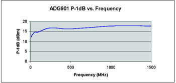
Figure 3. P1dB vs. frequency for the ADG901.
Traditional Switching Solutions:
1. Pin Diodes
A PIN diode is fundamentally a current-controlled resistor at radio and microwave frequencies. PIN diodes have commonly been used for switching RF signals, as they are highly linear when conducting and exhibit very good distortion characteristics. PIN diodes are fabricated by placing a high resistivity intrinsic (I) region between P-type and N-type silicon regions. The resistance value of the PIN diode is determined only by the forward-biased DC current, making it useful in switching functions. When a PIN diode is forward-biased, electrons and holes are injected from the P and N regions into the I region. The electrons and holes do not recombine immediately; instead a finite charge is stored, resulting in a lowering of the resistivity of the I region and allowing conduction. Typical values of resistance obtained for different bias currents are on the order of 0.1 ohm for 1 A up to 10 kohm for 1 µA.
Accordingly, the first drawback when using PIN diodes is that they require large amounts of DC power for low resistivity and low insertion loss. This is a huge disadvantage when they are used in portable equipment such as PDAs and handheld meters, since battery life is directly proportional to power consumption. It is also difficult to achieve more than 30 dB isolation at higher frequencies when using a single-series or shunt-connected PIN diode. To obtain higher levels of isolation, two or more diodes must be connected in a series-shunt combination. This has the undesirable effect of increasing insertion loss.
A typical transmit/receive (TX/RX) PIN diode switch schematic is shown in Figure 4. It consists of two diodes, some DC blocking capacitors, an inductor to feed the DC forward bias control signal, and some discrete components to create a quarter-wave line. If extra RF ports need to be switched, more series-connected diodes are required, which results in increased insertion loss. The effect of increased insertion loss in this application is twofold. On the TX side, every fraction of a decibel lost between the power amplifier and the antenna means that the TX signal needs more amplification, thus reducing battery life. On the RX side, an increase in insertion loss will serve to reduce the receive signal strength, degrading the overall signal-to-noise ratio (SNR) and receiver sensitivity.
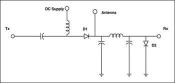
Figure 4. A typical TX/RX switch using PIN diodes.
Another limitation of PIN diodes is that they require an external driver to control the switching speed of the TX/RX switch and the interface levels that can be used.
2. GaAs Switches
In recent years, GaAs switches have dominated the wideband switch market due to their low DC power consumption (compared to PIN diodes). GaAs switches are made up of arrays of transistors that act as voltage-controlled resistors. The GaAs transistor is a three-terminal device; the gate voltage (Vg) controls the resistance between the other two terminals. To increase isolation between RF ports, they can be connected in series or as shunt devices to ground. Unlike PIN diodes, the placement of multiple transistors in series actually aids RF power-handling and linearity, with little effect on insertion loss. A typical TX/RX switch schematic is shown in Figure 5. Here, transistors are connected in a series-shunt configuration to obtain the optimum insertion loss and isolation performance. The drawback of this configuration is that complementary switching of MN1/MN4 and MN2/MN3 requires that both high and low logic levels be available simultaneously, increasing the complexity of the control circuitry and thus the cost.
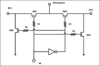
Figure 5. A typical transistor based TX/RX switch schematic.
MMIC GaAs switches are available from a wide variety of companies. All use an N-channel depletion-mode FET as the basic switching device. The characteristics displayed by these devices are as follows:
Vg = 0 —> Switch ON
Vg = Negative —> Switch OFF (Pinchoff)
Pinchoff is defined as the voltage at which the channel becomes high impedance. This usually occurs at Vg of –3 V, depending on the process used. RF levels at the input of the switch can modulate the Vg, thereby causing distortion products as the on resistance of the switch varies. The use of high control voltages will reduce this effect, but only at the cost of generating voltages of approximately +2 V to –8 V to control the switches. GaAs processes don’t offer complementary devices, so it takes a lot more current to create the inverter logic functions that are easily available in CMOS technology. This inherent liability of GaAs switches makes them hard to integrate into most modern electronic systems that use positive low voltage power supplies. GaAs switch manufacturers get around this issue by adding DC blocking capacitors in series with the RF pins of the switch. This effectively floats the die relative to DC ground, which allows the switches to be controlled with positive control voltages. The drawback, however, is that the DC blocking capacitors limit the bandwidth that the switches can handle, thus restricting their usage in wide band systems. The capacitors themselves are relatively cheap, but the additional printed circuit board area and manufacturing costs can significantly add to the overall switch cost. Also, any component placed in series with the switch will add to the insertion loss and have a direct impact on system SNR. Any increase in inductance or path length will degrade the performance of the devices, thus giving a system designer additional issues and problems to overcome.
As mentioned earlier, the control signals for the GaAs switch need to be generated from an external source. There are a number of methods to do this; the easiest and most common being the addition of an external CMOS driver IC. This extra IC not only draws power, but also adds to PC board area and assembly cost. More recently, GaAs switch manufacturers have introduced the MultiChip Module (MCM), which packages the CMOS/BiCMOS driver die and the GaAs switch die into one large BGA-type package. These MCMs work quite well, but have the major drawback of high overall solution cost, made up of the individual costs of both die, and the increased assembly cost due to the larger package and die interconnect.
CMOS to the Rescue
As Moore’s Law [1] has predicted, standard CMOS process geometries have continued to decrease. One of the markets that has opened up to CMOS is the area of RF/Microwave ICs. With reduced transistor lengths, CMOS has achieved low on resistance, low off capacitance and good linearity up to 1 GHz and beyond. This is the case for RF switches also, as CMOS switches with a 1 GHz, 3 dB bandwidth are now available.
Like GaAs switches, CMOS switches use NMOS FETs, which act essentially as voltage-controlled resistors. The characteristics displayed by these devices are as follows:
Vgs > Vt —> Switch ON
Vgs < Vt —> Switch OFF
Vt is defined as the threshold voltage above which a conducting channel is formed between the source and drain terminals. The FETs can have an interlocking finger layout to reduce the parasitic capacitance between the source and drain, thereby increasing isolation at high frequency.
As was stated previously, CMOS switches are suitable for many low-power applications. Their power handling capability is reduced as frequency is reduced for two reasons: first, the inherent NMOS structure as shown in Figure 6 consists of two regions of N-type material in a P-type substrate, which leads to parasitic diodes being formed between the N and P regions. When an AC signal, biased at 0 VDC, is placed on the source of the transistor, and Vgs is such that the transistor is turned on, the parasitic diodes can be forward-biased for some portion of the negative half cycle of the input waveform. Once the input sine wave goes below approximately –0.6 V, the diode will begin to turn on. This will cause the input signal to be compressed. At low frequency, the input signal is below the –0.6 V level for longer periods of time, thus having a greater impact on the 1 dB compression point (P1dB). The second mechanism is the partial turn-on of the shunt NMOS device when it is supposed to be off. As was mentioned previously, the NMOS transistor is in the off state with Vgs < Vt. With an AC signal on the source of the shunt device, there will be a time in the negative half cycle of the waveform where Vgs ≥ Vt, thereby partially turning on the shunt device. This will cause the input waveform to compress by shunting some of its energy to ground. Both of these mechanisms can be overcome by applying a small DC bias (~0.5 V) to the RF input signal when the switch is being used at low frequency (<30 MHz) and high power (>10 dBm). Unlike GaAs switches, DC blocking capacitors are not required with CMOS switches.
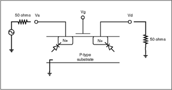
Figure 6. Physical NMOS structure.
Benefits of CMOS
There are a number of key benefits of using CMOS to design-wide bandwidth switches. The main advantages and key high performance specifications are highlighted in the following sections.
Cost: The most important advantage in today’s cost-driven market is that CMOS processes are significantly less expensive than GaAs processes, leading to a reduced die cost. CMOS switches use positive voltage control, and do not require DC blocking capacitors. GaAs transistors, on the other hand, are negative voltage controlled devices. This precludes the use of CMOS drivers, requires DC blocking capacitors to be used on the RF inputs, and causes an increase in the overall solution cost. CMOS switches are both less expensive and easier to use than their GaAs counterparts.
Single-pin Control Interface: CMOS switches have a single-pin control interface that enables maximum circuit layout efficiency, benefiting many applications such as mobile wireless systems. This is possible because CMOS allows the integration of driver/switch control circuitry onto the same die as the switches, effectively reducing the number of control pins. CMOS technology provides a control interface that has a simple single-pin control in contrast to the complementary control signals implemented by many GaAs RF switches. As an example, for an SPDT (Single Pole Double Throw) switch, a GaAs part needs two control lines whereas a CMOS device requires only one.
Easy System Integration: The on-chip driver on CMOS switch technology can interface with both TTL and CMOS logic levels, allowing the parts to easily integrate with other CMOS/BiCMOS ICs such as microcontrollers. Control inputs that are both CMOS and LVTTL compatible provide a very simple interface in many applications.
There is no need for the addition of DC blocking capacitors on the RF inputs for CMOS switches, eliminating concerns over reduced bandwidth or the impact of reduced system performance—reasons which were described in the previous section.
Reduced Package Size: The easy integration of driver/switch control circuitry has the added benefit of small package size. The overall size of the CMOS die is smaller, allowing CMOS devices to be assembled in smaller packages with lower pin counts than the MCMs being offered by GaAs manufacturers. A standard SPDT switch pin count can range from a modest 8-pin package for a CMOS solution up to 20 pins for a GaAs solution.
This space saving is even more obvious for SP4T devices. CMOS devices are available in tiny 16-lead 3 mm × 3 mm LFCSP (Lead Frame Chip Scale Package) sets. GaAs SP4T products can require negative or positive/negative voltage supplies, and up to eight control lines. They are packaged in 24-lead 10.65 mm × 15.6 mm wide body SOIC (Small Outline) or 28-pin 12.57 mm × 12.57 mm PLCC (Plastic Leaded Chip Carrier) packages.
Lower Power Consumption: The extremely low power consumption of CMOS switches makes them ideally suited to portable applications.
Available CMOS RF switches operate from a single 1.65 V to 2.75 V supply, and have typical current consumption of less than 1 µA—significantly lower than that specified for an equivalent GaAs solution.
Other CMOS Switching Performance highlights: Matching is also very good for CMOS switches. Figure 7 shows a typical plot of return loss versus frequency for an on/off switch. This plot shows that the S11 values are 27 dB out to 100 MHz and 26 dB at 1 GHz for the on switch and 23 dB out to 100 MHz and 20 dB at 1 GHz for the off switch. This is the amount of reflected power relative to the incident power at a port. A large return loss indicates good matching. CMOS switches have the additional flexibility of offering the use a choice of reflective (0 ohm) or absorptive (50 ohm) versions, allowing the switch to be matched to the application. For example, the ADG918 is an absorptive (or matched) SPDT switch (2:1 Mux) having 50 ohm terminated shunt legs, and the ADG919 is a reflective SPDT switch that has a direct shunt to ground. An absorptive switch would be preferred for applications where impedance matching is most critical. Similar to the off isolation performance of CMOS switches described earlier, the return loss specified for CMOS processes outperforms many GaAs switches by about 10 dB/decade.
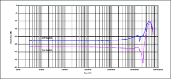
Figure 7. Return loss vs. frequency (off/on switch) for ADG918.
Switching time is also excellent, with CMOS switches featuring a typical switching time of 5 ns—up to ten times faster than many GaAs parts. Figure 8 shows the 5 ns switching time of a typical ADG901. The timing specifications of this part at extreme temperature conditions are 8 ns maximum, compared with microseconds for many
GaAs switches.
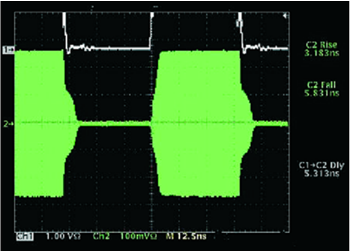
Figure 8. Switch Timing for the ADG901.
Conclusion
CMOS switches present a simpler overall solution than GaAs devices for high frequency switching requirements, with the added benefit of lower cost.
The ADG9xx family of wideband CMOS switches have a 3 dB frequency greater than 3 GHz, exhibit very low insertion loss of 0.8 dB at 1 GHz, and have greater than 37 dB isolation at 1 GHz. Such characteristics make these parts ideal for many applications from DC to 1 GHz and beyond. The switches offer a major CMOS challenge to GaAs RF switches and are the best solution for low power, high performance, high frequency switching applications.
Note
1. Moore’s Law predicted that the number of transisters per square inch on integrated circuits would double every year after the invention of the integrated circuit and that this trend would continue for the foreseeable future.


