CMOS Op Amp Outperforms Bipolar Amps in Precision Applications
Introduction
The LTC6081 and LTC6082 are dual and quad low offset, low drift, low noise CMOS operational amplifiers with rail-to-rail input and output stages. Their 0.8µV/°C maximum offset drift, 1pA input bias current,1.3µVp-p of 0.1Hz to 10Hz noise, 120dB open loop gain and 110dB CMRR and PSRR make them perfect for precision applications. The LTC6081 and LTC6082 have a gain bandwidth product of 3.6MHz, with each amplifier only consuming about 330µA current for a supply voltage of 2.7 to 5.5V. The 10-lead DFN package of the LTC6081 offers a shutdown function to reduce each amplifier’s supply current to 2µA.
Superior Precision CMOS Op Amp
Bipolar amplifiers can have low offset and low offset drift, but their nA level input bias current make them inappropriate for high input impedance applications such as photodiode amplifiers. CMOS amplifiers usually offer inferior offset drift, CMRR, and PSRR specifications and therefore are not suitable for precision applications. Chopper stabilized amplifiers, also known as zero drift amplifiers, can achieve superior offset and offset drift by means of offset cancellation, but have clock noise and fold-back noise due to sampling. LTC6081 and LTC6082, however, are continuous time CMOS operational amplifiers, which use a patented methodology to improve their offset voltage, offset voltage drift and CMRR. They combine the features of low input bias current, low offset drift and low noise.

Figure 1. VOS drift histogram of LTC6081
Instrumentation Amplifier
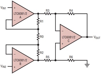
Figure 2 shows a typical three op amp instrumentation amplifier. If R1 = R2, R3 = R5 and R4 = R6, then


Figure 2. Typical three op amp structure of instrumentation amplifier
In this two stage structure, the differential voltage passes through the first gain stage with gain of 1 + 2 R1/R0 while the common mode voltage has only unity gain at the first stage, thus improving CMRR. Ratio matching of R4/R3 and R6/R5 is critical for CMRR. Gain can be changed by simply changing R0 without affecting the resistor matching.
The input referred offset of the amplifier is

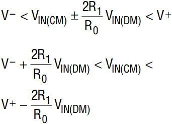
Statistically, the total VOS is √2 times the VOS of a single op amp. Since a single LTC6081 op amp drifts less than 0.8µV/°C, the amplifier in Figure 2 will drift less than 1.1µV/°C. One drawback of the circuit in Figure 2 is its common mode operating range is no longer rail-to-rail. Assuming the differential and common mode input voltage are VIN(DM) and VIN(CM) respectively, the output voltages of op amp A and B are then VIN(CM) – (2R1/ R0)VIN(DM) and VIN(CM) + (2R1/R0)VIN(DM) respectively. So

where V+ and V– are the positive and negative supply voltage respectively. The larger the first stage gain or input differential signal is, the narrower the input common mode range is. To widen the input common mode range, the first stage gain can be reduced, but this will compromise CMRR performance.
Figure 3 is a reduced circuit of Figure 2 with a unity gain buffer at the front stage. This circuit can achieve rail-to-rail input range. As mentioned previously, it won’t have the high CMRR of the circuit in Figure 2 since we reduced the front stage gain to unity. If the input resistance requirement can be eased, Figure 3 can be reduced to Figure 4, a single stage difference amplifier. The impedance of the non-inverting and inverting inputs are R3 and R5 + R6, respectively. An obvious advantage of the LTC6081 is its super low input bias current. Even with a 1MΩ input resistor R3 or R5, the less than 1pA input bias current of LTC6081 will add less than 1µV to VOS.

Figure 3. Instrumentation amplifier with unity gain buffers

Figure 4. Difference amplifier with no input buffers
The above discussion assumes a perfect matching of R4/R3 and R6/R5. If

then the CMRR degrades to

where AV is the differential gain of the instrumentation amplifier. For example, at gain of 10, to achieve 80dB CMRR, mismatch of R4/R3 and R6/R5 should be less than 0.1%. This is true for all the above three circuits. The advantage of the circuit in Figure 2 is that gain can be put at the front stage to ease the matching requirements of the second stage. Matching of R1 and R2 in Figure 2 is not important.
Thermocouple Amplifier
Figure 5 shows the LTC6081 in a thermocouple amplifier. The 1MΩ resistors protect the circuit up to ±350V with no phase reversal to amplifier output. The 1pA maximum IBIAS of the LTC6081 translates to a minuscule 0.05°C temperature error with the 1MΩ input protection resistor. The ±90µV offset over the entire operating temperature range ensures a less than 2°C temperature offset.

Figure 5. Thermocouple amplifier
Conclusion
The LTC6081 and LTC6082 are high performance dual and quad op amps combining excellent noise, offset drift, CMRR, PSRR and input bias current specifications. They perform in a variety of topologies without compromising performance. LTC6081 is available in 8-lead MSOP and 10-lead DFN packages. LTC6082 is available in 16-lead SSOP and DFN packages.


