Digital feedback occurs when the high speed transitions at the outputs of a high speed ADC are coupled (either capacitely or inductively) through the ground plane back to the sensitive analog input, creating unwanted tones and impairing the performance of the ADC. For a differential input ADC, the most problematic area for digital feedback is when there is a small analog input signal centered around mid-scale. In those cases, the digital outputs toggle between mostly 1’s and mostly 0’s for both binary and two's complement output data, resulting in a majority of outputs toggling simultaneously (see below). The simultanous switching of a large number of high speed digital outputs causes a large change in the ground plane current and this ground plane noise can appear as digital feedback noise.


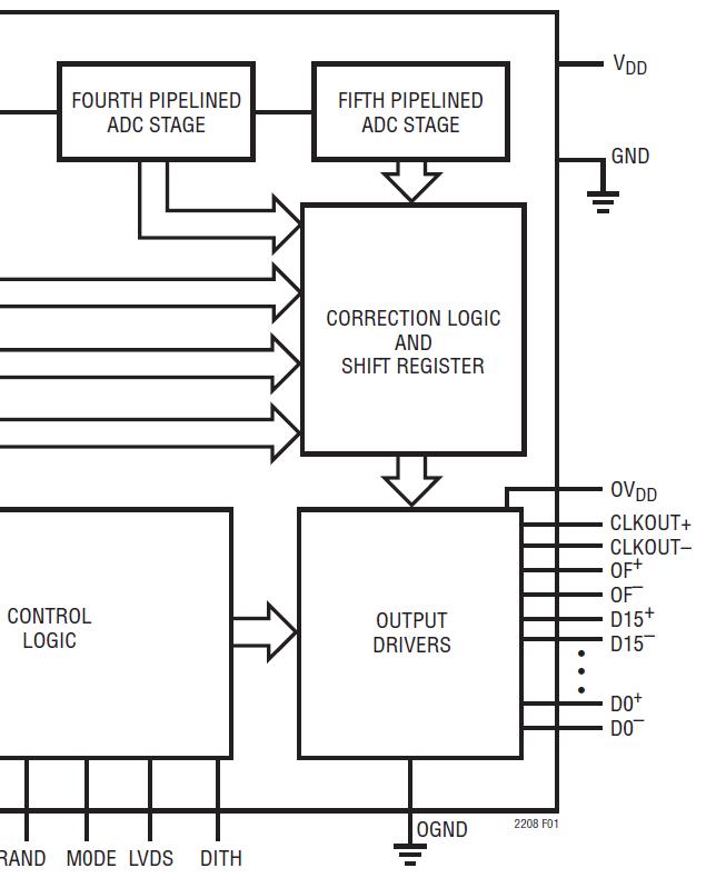
Alternate bit polarity mode is a feature of some high speed analog-to-digital converters (ADCs) that can reduce the effect of digital feedback on a circuit board. By inverting every other bit, alternate bit polarity mode minimizes the change in current flow in the ground plane at the midscale transition point, thereby reducing digital current noise. When alternate bit polarity mode is enabled, all of the odd output data bits (D1, D3, D5, D7, D9, D11, D13) shown in the figure below from the LTC2208 16-bit 130Msps ADC data sheet (the LTC2208 provides the option of CMOS or parallel LVDS outputs) are inverted before the output buffers. The even bits (D0, D2, D4, D6, D8, D10, D12), the overflow bit (OF) and the output clock signal (CLKOUT) are not affected.

Note that there will still be a code transition that cause the outputs to change from all (or mostly) ones to all (or mostly) zeroes, but the transition no longer occurs around the more noise-sensitive midscale point.
When using alternal bit polarity mode, the digital output needs to be decoded at the receiver (the user's FPGA/microporcessor) by inverting the odd bits (D1, D3, D5, D7, D9, D11, D13). Alternate bit polarity mode is independent of another technique that minimizes digital feedback, namely the digital output randomizer mode. Either or both functions can be enable at the same time. Alternate bit polarity mode is enabled by setting the appropriate bit in the ADC's internal programming control register.
この記事に関して
製品


