A 7ns, 6mA, Single-Supply Comparator Fabricated on Linear’s 6GHz Complementary Bipolar Process
A 7ns, 6mA, Single-Supply Comparator Fabricated on Linear’s 6GHz Complementary Bipolar Process
1998年05月01日
Introduction
The LT1394 is an ultrafast (7ns), low power (6mA), single-supply comparator designed to operate on either 5V or ±5V supplies. It has a maximum offset voltage of 2.5mV, complementary TTL compatible outputs and output latch capability. The LT1394 is the first product made with Linear Technology’s 6GHz complementary bipolar technology. This fine-line geometry process results in a product with dramatically improved speed and power compared to industry-standard comparators developed in slower NPN-only technologies.
These features combine to make the LT1394 well suited for applications such as high performance NTSC crystal oscillators, single-supply voltage-to-frequency converters and high speed, high accuracy level detectors. The LT1394 is offered in SO-8 and is pin compatible with the industry-standard LT1016 and LT1116 comparators.
Circuit Description
A simplified schematic of the LT1394 can be seen in Figure 1. There are differential inputs (+IN/–IN), differential outputs (OUT/OUT), a latch input (LATCH) and three power supply pins (VEE, VCC and GND). The circuit topology consists of a differential input stage, a level-shifting gain stage, a latch stage and complementary output stages. The complementary output stages offer improved flexibility for the user; the latch stage provides superior sampling accuracy of the input signal without the need for an external latch.
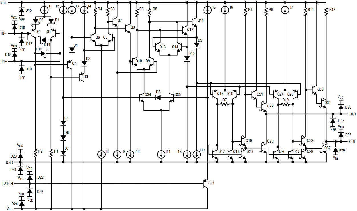
Figure 1. LT1394 simplified schematic.
The input stage of the LT1394 uses a PNP differential pair (Q1–Q2) with Schottky diodes in the emitters (D1–D2) and resistive loads (R1–R2). The Schottky diodes in series with the emitters allow differential input voltages that are greater than the base-emitter breakdown of the input transistors. Two additional Schottky diodes (D11–D12) prevent output phase reversal when either input is taken far enough below VEE to forward bias the base-collector junction of its corresponding PNP input transistor. To allow single-supply operation, the input stage has been designed to have small voltage swings across load resistors R1 and R2. This ensures that the input PNPs will not saturate with the LT1394 inputs at VEE.
The signal path remains differential as it is buffered and level shifted via transistors Q3–Q4 and diodes D3–D4. The level shift prevents current source I8 from saturating. The second gain stage, comprising transistors Q5–Q6 and resistors R3–R4, takes additional gain while level shifting the signal back to VCC. The differential output of the second gain stage is buffered by transistors Q7–Q8, which then drive the latch stage.
In the latch stage, transistors Q9–Q10 and resistors R5–R6 act as a third gain stage. Q11–Q12 buffer the signal at resistors R5–R6, driving another differential pair (Q13–Q14). Q13 and Q14, when activated, provide positive feedback to resistors R5–R6, creating the latch. When the LATCH pin is low, the LT1394 is in flow-through or GAIN mode. Current I11 is steered through Q34, activating the Q9–Q10 differential pair. When the LATCH pin is high, the LT1394 is in LATCH mode. Current I11 is steered through Q35, activating the Q13–Q14 differential pair. The output of the gain/latch stage has additional level shifting from the emitters of transistors Q11–Q12 via diodes D9–D10. This level shifting prevents the output stage current sources I6 and I7 from saturating.
The LT1394 provides complementary outputs by using two identical output stages connected in opposite phases. Examining the output circuitry for the OUT pin, a PNP differential pair (Q15–Q16) is driven from the outputs of the latch stage. When I6’s current is steered through Q16, it drives R7 and the base of Q19. R7 improves switching speed by reducing the gain of the differential pair Q15–Q16 and lowering the impedance at the base of Q19. Q19’s emitter current then drives the base of Q23, turning it on until the OUT pin has been pulled low and Q23’s Schottky clamp diode has turned on. Conversely, if I6’s current is steered through Q15, it allows R8 to pull up the Darlington-connected output transistors Q21 and Q22, bringing the OUT pin high. For faster output switching times, Q15’s collector current flows into the Q17/Q18/Q20 current mirror. Q20’s collector current helps turn off Q23, whereas the collector current of Q18 helps turn off Q19.
Linear Technology’s 6GHz Complementary Bipolar Technology
Linear Technology’s 6GHz complementary bipolar technology (6GHz ComBi) features vertical NPN and PNP transistors with similar frequency response and gain characteristics. Both the NPN and PNP transistors feature polysilicon emitters for improved gain, a collector-to-emitter breakdown voltage (BVCEO) greater than 12V and a unity gain frequency (fT) of 6GHz. The PNP transistors have a nominal current gain (β) of about 45, while the NPNs have a β of about 100.
In addition to the transistors, the 6GHz ComBi technology includes diode, resistor and capacitor structures. Schottky barrier diodes with low parasitic capacitance and high breakdown voltage are included for high speed voltage clamping and breakdown protection of transistors. Low parasitic capacitance polysilicon resistors are included for use in high speed signal paths. High resistivity diffused resistors are used for biasing and low power circuitry. Polysilicon-oxide-metal capacitors offer low parasitic capacitance, high capacitance density and low series resistance for good high frequency performance.
When compared to a typical 30V complementary bipolar process, the reduction of transistor BVCEO from 30V to 12V has many benefits for applications that do not require higher supply voltages. Dramatically reduced depletion widths within the transistor allow a 50% decrease in area. This area reduction improves speed by lowering parasitic capacitances associated with the transistor. The reduced voltage requirement also allows a thinner, richer epitaxial (epi) region. This change to the epi region dramatically reduces the collector resistance of the transistors, resulting in smaller transistors for a given current level. With this significant reduction in transistor size, interconnects using a single metallization layer becomes much more difficult and would generate significant parasitic capacitance. Because of this, the 6GHz ComBi process utilizes two levels of metallization.
Applications
4× NTSC Voltage-Tunable Crystal Oscillator
The first of three representative applications for the LT1394 can be seen in Figure 2. This circuit is a crystal oscillator with voltage tuning of the output frequency. This application makes use of the LT1394’s high speed, complementary outputs and single-supply 5V operation. Such voltage controlled crystal oscillators (VCXO) are often employed where slight variation of a stable carrier is required. This example is specifically intended to provide a 4× NTSC subcarrier tunable oscillator suitable for phase locking.
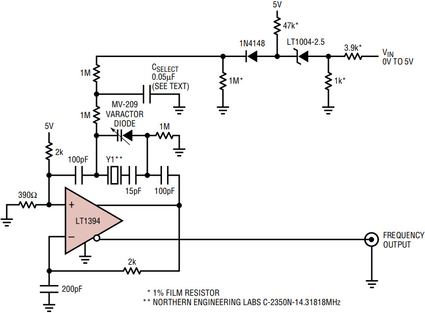
Figure 2. A 4× NTSC subcarrier voltage tunable crystal oscillator; tuning range and bandwidth accommodate a variety of phase-locked loops.
The resistors at the LT1394’s positive input set a DC bias point of 840mV. The 2kΩ– 200pF path sets up phase-shifted negative feedback, putting the DC output in the active region with a gain of 35 at the oscillation frequency. The crystal’s path provides resonant positive feedback and stable oscillation occurs. The varactor diode is biased from the tuning input. The tuning network is arranged so that a 0V to 5V drive provides a reasonably symmetric, broad tuning range around the 14.31818MHz center frequency. The capacitor labeled CSELECT sets the tuning bandwidth. It should be picked to complement loop response in phase-locking applications. Figure 3 is a plot of frequency deviation versus tuning input voltage. Tuning deviation from the 4× NTSC 14.31818MHz center frequency exceeds ±240ppm for a 0V to 5V tuning range.
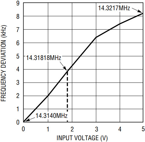
Figure 3. Control voltage vs output frequency for Figure 2; tuning deviation from the center frequency exceeds ±240ppm.
Simple 10MHz Single-Supply V/F Converter
A second application for the LT1394 is shown in Figure 4. It is a simple 10MHz single-supply voltage-to-frequency converter that makes use of the LT1394’s speed, single-supply operation and complementary outputs. A 0V to 2.5V input produces a 0Hz to 10MHz output with 40dB of dynamic range, 1% linearity and 400 ppm/°C gain drift. Power supply rejection is 0.5% for 4.75V to 5.25V supply excursions.
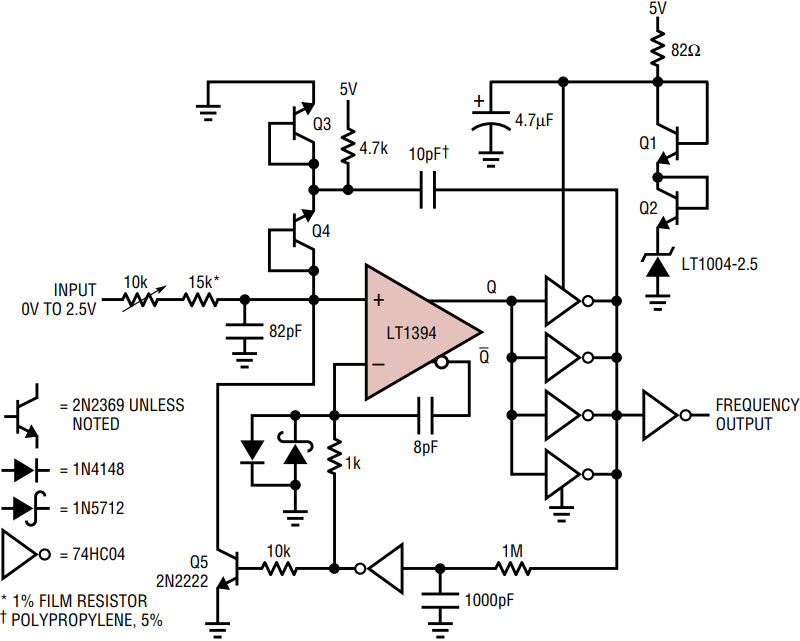
Figure 4. This simple charge pump-based 10MHz voltage-to-frequency converter has 40dB dynamic range and operates from a 5V supply.
To understand circuit operation, assume the LT1394’s positive input is slightly below its negative input. The circuit’s input voltage causes a positive-going ramp at the comparator’s positive input (Trace A, Figure 5). The Q output is low, forcing the CMOS inverter outputs high. This allows current flow from diode Q1’s collector, through the CMOS inverter supply pin, to the 10pF capacitor. The 4.7µF capacitor provides high frequency bypass, maintaining low impedance at Q1’s collector. Diode connected Q3 provides a path to ground. The voltage to which the 10pF capacitor charges is a function of Q1’s collector potential and Q3’s drop. When the ramp at the comparator’s positive input goes high enough, the Q output goes high and the paralleled inverters switch low (Trace B). This action pulls current from the 82pF capacitor at the input via the Q1–10pF route (Trace D). This current removal resets the LT1394’s positive input ramp to a potential slightly below ground, forcing the Q output low and the paralleled inverters high. The 8pF capacitor at the LT1394’s inverting output furnishes AC positive feedback to the negative input (Trace C). This ensures that the Q output remains high long enough for a complete discharge of the 10pF capacitor. The Schottky diode prevents the LT1394’s input from being driven outside its negative common mode limit. When the 8pF capacitor’s feedback decays, the LT1394 again switches and the entire cycle repeats. The oscillation frequency depends entirely upon the input-derived current. The LT1004 is the circuit’s voltage reference, with Q1 and Q2 temperature compensating Q3 and Q4.
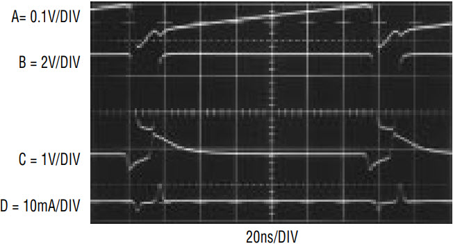
Figure 5. Waveforms for the 10MHz voltage-to-frequency converter; charge pump-based feedback provides linearity and fast response to input.
Start-up or overdrive can cause the circuit’s AC-coupled feedback to latch. If this occurs, the LT1394’s output goes high, causing the paralleled inverters to go low. After a time determined by the 1MΩ–1000pF RC, the associated lone inverter goes high. This lifts the LT1394’s negative input and grounds the positive input with Q5, initiating normal circuit action.
To calibrate this circuit, apply 2.5V and adjust the 10k potentiometer for a 10MHz output.
18ns 500µV Level Detector
The ultimate limitation on comparator sensitivity is available gain. Unfortunately, increasing gain invariably involves giving up speed. The gain vs speed trade-off in fast comparators is usually a practical compromise designed to satisfy most applications. Some situations, however, require more sensitivity (that is, higher gain) with minimal effect on speed. Figure 6’s circuit adds a differential preamplifier ahead of the LT1394, increasing gain. This permits 500µV comparisons in 18ns. A parallel-path DC stabilization approach eliminates preamplifier drift as an error source. A1 is the differential amplifier, operating at a gain of 100. Its output is AC coupled to the LT1394. A1 has poorly defined DC characteristics, necessitating some form of DC correction. A2 and A3, operating at a differential gain of 100, provide this function. They differentially sense a band-limited version of A1’s inputs and feed DC and low frequency amplified information to the comparator. The low frequency roll-off of A1’s signal path complements A2–A3’s high frequency roll-off. The summation of these two signal channels at the LT1394’s inputs results in flat response from DC to high frequency.
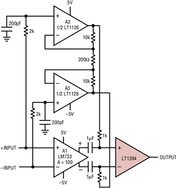
Figure 6. Parallel preamplified paths allow 18ns response to 500µV overdrive.
Figure 7 shows waveforms for the high sensitivity level detector. Trace A is a 500µV overdrive on a 1mV step applied to the circuit’s positive input (negative input grounded). Trace B shows the resulting amplified step at A1’s positive output. Trace C is A2’s band-limited output. A1’s wideband output combines with A2’s DC-corrected information to yield the correct, amplified composite signal at the LT1394’s positive input in Trace D. The LT1394’s output is Trace E. Figure 8 details circuit propagation delay. The output responds in 18ns to a 500µV overdrive on a 1mV step. Figure 9 plots response time versus overdrive. As might be expected, propagation delay decreases at higher overdrives. A1’s noise limits usable sensitivity.
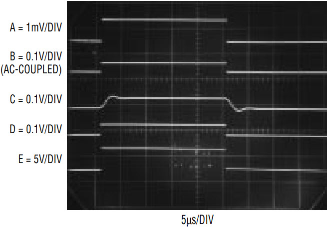
Figure 7. 500µV input (Trace A) is split into wideband and low frequency gain paths (Traces B and C) and recombined (Trace D). Trace E is the level-detector output.
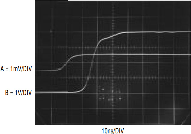
Figure 8. Parallel-path level detector shows 18ns response (Trace B) to 500µV overdrive (Trace A).
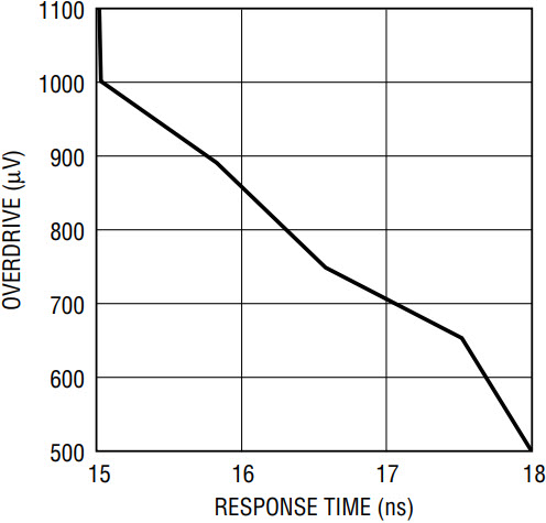
Figure 9. Response time vs overdrive for the composite level detector.
Conclusion
Innovative circuit design, coupled with Linear Technology’s 6GHz complementary bipolar process simultaneously achieves the seemingly contradictory goals of high speed and low power. The LT1394 is easy to use, thanks to its single-supply capability and complementary outputs. Additional LT1394 applications appear in the forthcoming Linear Technology Application Note, A Seven Nanosecond Comparator for Single Supply Operation.
著者について
James M. Williams(1948年4月14日~2011年6月12日)はマサチューセッツ工科大学(1968年~1979年)、Philbrick、National Semiconductor(1979年~1982年)、Linear Technology Corporation(LTC)(1982年~2011年)でアナログ回路設計者ならびに技術文書の著者を務めていました。同氏は、書籍5冊、National Semiconductorの...


