60 GHz Line of Sight Backhaul Links Ready to Boost Cellular Capacity
A complete 60 GHz two-way data communication scheme based on the Xilinx® Zynq SoC and ADI V-band chipset offers the performance and flexibility to serve the small cell backhaul market.
The ever increasing demand for data on the world’s cellular networks has operators searching for ways to increase the capacity 5000 fold by 2030.1 Getting there will require a 5× increase in channel performance, a 20× increase in allocated spectrum, and a 50× increase in the number of cell sites.
Many of these new cells will be placed indoors where the majority of traffic originates and fiber is the top choice to funnel the traffic back into the networks. But there are many outdoor locations where fiber is not available or is too expensive to connect, and for these situations wireless backhaul is the most viable alternative.
Unlicensed spectrum at 5 GHz is available and does not require a line of sight (LOS) path. However, the bandwidth is limited and interference from other users of this spectrum is almost guaranteed due to heavy traffic and wide antenna patterns.
Communication links of 60 GHz are emerging as a leading contender to provide these backhaul links for the many thousands of outdoor cells that will be required to meet capacity demands. This spectrum is also unlicensed, but unlike frequencies below 6 GHz, it contains up to 9 GHz of available bandwidth. Moreover, the high frequency allows for very narrow and focused antenna patterns that are somewhat resistant to interference, but require LOS paths.
FPGA-based and SoC-based modems are increasingly being used in various wireless backhaul solutions since platforms using them can be modular and customizable, thereby reducing the total cost of ownership for OEMs. For the radio portion of these links, transceivers have been integrated into silicon-based ICs and packaged into low cost, surface-mount parts.
Commercial parts are available to build a complete 60 GHz two-way data communication link as exemplified by the solution in Figure 1. Developed by Xilinx and Hittite Microwave (now part of Analog Devices), the design includes a Xilinx modem and an Analog Devices millimeter wave radio. This link meets the performance and flexibility requirements of the small cell backhaul market.
As depicted in Figure 1, two nodes are required to create this link. Each node contains a transmitter (with a modulator) and its associated analog transmitter chain, and a receiver (with a demodulator) and its associated analog receiver chain.
The modem card is integrated with analog and discrete devices. It contains oscillators implemented digitally to ensure the accuracy of frequency synthesis, and all the digital functions are executed in an FPGA or system on chip (SoC). This single-carrier modem core supports modulations from QPSK to 256 QAM in channel bandwidths up to 500 MHz and achieves data rates as high as 3.5 Gbps. The modem also supports both frequency division duplex (FDD) and time division duplex (TDD) transmission schemes. Robust modem design techniques reduce the phase noise implications of the local oscillators. Powerful low density parity check (LDPC) coding is included for improved performance and link budget.
Millimeter Wave Modem
The millimeter wave modem enables infrastructure vendors to develop flexible, cost optimized, and customizable links for their wireless backhaul networks. It’s fully adaptive, low in power, small in footprint, and can be used to deploy indoor and full outdoor point-to-point links as well as point-to-multipoint microwave links. The solution presents operators with the ability to build scalable and field upgradable systems.
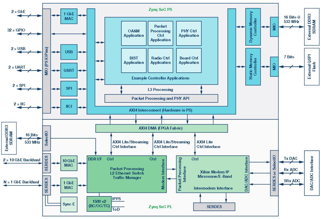
Figure 2 further details the digital modem, as implemented in an SoC-based solution. Besides the programmable logic (PL), the platform’s scalable processing system (PS) contains dual ARM® Cortex®-A9 cores with integrated memory controllers and multistandard I/Os for peripherals.
This SoC platform is used to perform various data and control functions and to enable hardware acceleration. An integrated millimeter wave modem complete with PHY, controller, system interfaces, and a packet processor is shown in Figure 2. However, based on the required architecture, you could insert, update, or remove different modules. For instance, you might choose to implement an XPIC combiner so that you could use the modem in cross polarization mode with another modem. The solution is implemented in the PL, where SERDES and I/Os are used for various data path interfaces such as those between the modem and packet processor, the packet processor and memory, or the intermodem or DAC/ADC.
Some of the other important features of the modem IP include automatic hitless and errorless state switching through adaptive coding and modulation (ACM) to keep the link operational; adaptive digital closed-loop predistortion (DPD) to improve RF power amplifier efficiency and linearity; synchronous Ethernet (SyncE) to maintain clock synchronization and Reed-Solomon or LDPC forward error correction (FEC). The FEC choice is based on the design requirements. LDPC FEC is the default choice for wireless backhaul applications, whereas Reed-Solomon FEC is preferred for low latency applications such as fronthaul.
LDPC implementation is highly optimized and exploits FPGA parallelism for computations done by the encoders and decoders. The result is noticeable SNR gains. You can apply different levels of parallelism by varying the number of iterations of the LDPC core, thereby optimizing the size and power of the decoder. You can also model the design based on channel bandwidth and throughput constraints.
This modem solution also comes with a graphical user interface (GUI) for both display and debug, and it is capable of high level functions such as channel bandwidth or modulation selection, as well as low level functions, such as setting of hardware registers. To achieve 3.5 Gbps throughput for the solution shown in Figure 1, the modem IP runs at a 440 MHz clock rate. It uses five gigabit transceivers (GTs) for connectivity interfaces to support ADCs and DACs and a few more GTs for 10 GbE payloads or CPRI interfaces.
Millimeter Wave Transceiver Chipset
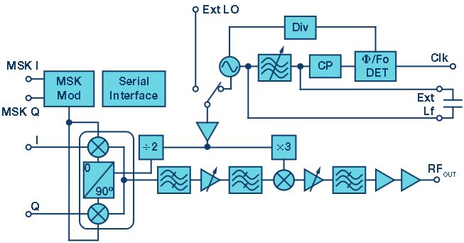
Analog Devices optimized its second-generation, silicon-germanium (SiGe) 60 GHz chipset used in this design for small cell backhaul applications. The transmitter chip is a complete analog baseband to millimeter wave upconverter. An improved frequency synthesizer covers 57 GHz to 66 GHz in 250 MHz steps with low phase noise that can support modulations of up to at least 64 QAM. Output power has increased to roughly 16 dBm linear power, while an integrated power detector monitors the output power so it does not exceed the regulatory limits.
The transmitter chip offers either analog control or digital control of the IF and RF gains. Analog gain control is sometimes needed when using higher order modulations since discrete gain changes can be mistaken for amplitude modulation, leading to bit errors. A built-in SPI interface supports digital gain control.
For applications requiring even higher order modulation in narrow channels, an external PLL/VCO with even lower phase noise can be injected into the transmitter, bypassing the internal synthesizer.
Figure 3 shows a block diagram of the transmitter chip, which supports up to 1.8 GHz of bandwidth. An MSK modulator option enables low cost data transmissions up to 1.8 Gbps without the need for expensive and power hungry DACs.
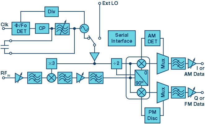
Complementing this device is a receiver chip, likewise optimized to meet the demanding requirements of small cell backhaul applications. The receiver features a significant increase in the input P1dB to −20 dBm and IIP3 to −9 dBm to handle short range links where the high gain of the dish antennas leads to high signal levels at the receiver input.
Other key features include a low 6 dB noise figure at the maximum gain settings; adjustable low-pass baseband filters and high-pass baseband filters; the same new synthesizers as found in the transmitter chip to support 64 QAM modulation over the 57 GHz to 66 GHz band and either analog or digital control of the IF and RF gains.
A block diagram of the receiver chip is shown in Figure 4. Note that the receiver also contains an AM detector to demodulate amplitude modulations such as on/off keying (OOK). Also, an FM discriminator demodulates simple FM or MSK modulations. This is in addition to the I/Q demodulator that is used to recover the quadrature baseband outputs for QPSK and more complex QAM modulations.
Both transmitter and receiver come in a 4 mm × 6 mm BGA style, wafer level package. These surface-mount parts will enable low cost manufacturing of radio boards for backhaul applications.
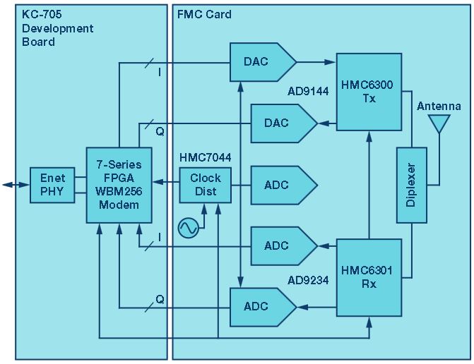
A block diagram of an example millimeter wave modem and radio system is shown in Figure 5. In addition to the FPGA, modem software, and millimeter wave chipset, the design also contains a number of other components. They include a dual-channel, 12-bit, 1 GSPS ADC, a quad-channel 16 bit, up to 2.8 GSPS TxDAC, and an ultralow jitter clock synthesizer with support for the JESD204B serial data interface employed on both the ADC and DAC ICs.
Demonstration Platform
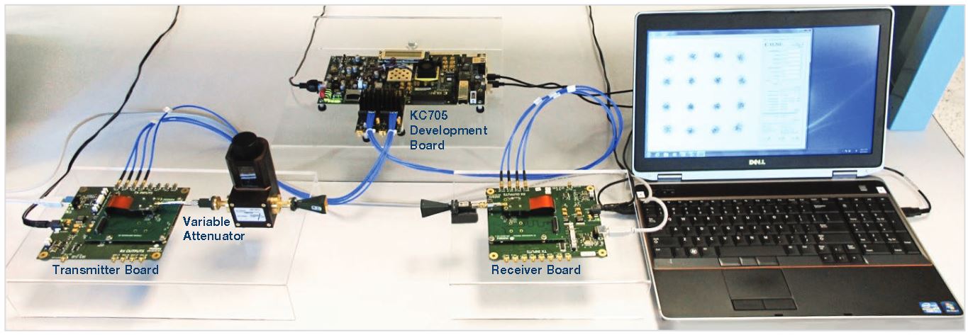
The platform shown in Figure 6 was jointly created by Xilinx and Analog Devices to be used for demonstration purposes. This implementation includes the FPGA-based modem on a Xilinx development board, an industry-standard FMC board containing ADCs, DACs, clock chip, and two radio module evaluation boards.
The demo platform includes a laptop for modem control and visual display and a variable RF attenuator to replicate the path loss of a typical millimeter wave link. The FPGA on the development board executes the WBM256 modem firmware IP. An industry-standard FMC mezzanine connector on the development board is used to connect to the baseband and millimeter wave radio boards.
The millimeter wave modules snap onto the baseband board. The modules have MMPX connectors for the 60 GHz interfaces as well as SMA connectors for optional use of an external local oscillator.
This platform contains all the hardware and software needed to demonstrate point-to-point backhaul connections of up to 1.1 Gbps in 250 MHz channels for each direction of a frequency division duplex connection.
Modular and Customizable
Since they’re highly modular and customizable, FPGAs can reduce cost when used to build platforms for wireless backhaul applications. When choosing commercial parts for a millimeter wave modem solution for the small cell backhaul market, select power efficient FPGAs/SoCs and high performing wideband IP cores. High speed is also a factor to consider when selecting GTs for wideband communications and switching functions. Look for a solution that can scale to support multiple product variations, from lower end, small cell backhaul products operating at a few hundred megabits per second to 3.5 Gbps, on the same hardware platform.
For the radio portion, transceiver ICs packaged in surface-mount parts will lower the cost of manufacturing. Parts on the market will meet power, size, flexibility, and functionality requirements for wireless backhaul needs of small cell deployments. Also available for purchase are high performing data converters and clock management ICs equipped to complete a wire-less backhaul link.

