2.5A, 4MHz Monolithic Synchronous Regulator Offers a High Efficiency, Compact Solution by Reducing External Component Count and Size
2.5A, 4MHz Monolithic Synchronous Regulator Offers a High Efficiency, Compact Solution by Reducing External Component Count and Size
著者
Joey Esteves
2002年08月01日
Introduction
The LTC3412 offers a compact and efficient voltage regulator solution for portable electronics that require low supply voltages (down to 0.8V) from a 3.3V to 5V power bus. Internal power MOSFET switches, with only 85mΩ on-resistance, allow the LTC3412 to deliver up to 2.5A of output current with efficiency as high as 95%. The LTC3412 saves space by operating with switching frequencies as high as 4MHz, permitting the use of small inductors and capacitors.
The LTC3412 employs a constant frequency, current mode architecture that operates from an input voltage range of 2.625V to 5.5V and provides an adjustable regulated output voltage from 0.8V to 5V while delivering up to 2.5A of output current. The switching frequency can be set between 300kHz and 4MHz by an external resistor. The LTC3412 can also be synchronized to an external clock, where each switching cycle begins at the falling edge of the external clock signal. Since output voltage ripple is inversely proportional to the switching frequency and the inductor value, a designer can take advantage of the LTC3412’s high switching frequency to use smaller inductors without compromising output voltage ripple. Lower inductor values translate directly to smaller physical inductor case sizes, reducing the overall size of the system.
OPTI-LOOP® compensation allows the transient response to be optimized over a wide range of loads and output capacitors, including ceramics. For increased thermal handling, the LTC3412 is offered in a 16-lead TSSOP package with an exposed pad to facilitate heat sinking.
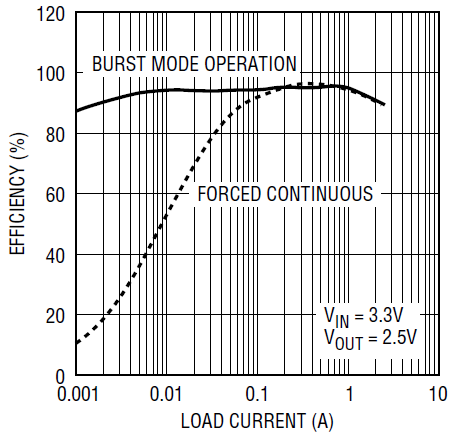
The LTC3412 can be configured for either programmable Burst Mode® operation or Forced Continuous operation. For portable battery-powered applications, Burst Mode operation extends battery life by reducing gate charge losses at light loads—at no load, the LTC3412 consumes a mere 62µA of supply current. Forced Continuous operation, though not as efficient as Burst Mode operation at light loads, maintains a steady operating frequency, making it easier to reduce noise and RF interference—important for some applications.
The LTC3412 provides for external control of the burst clamp level, in effect allowing the burst frequency to be varied. Lower Burst Mode operating frequencies result in improved light load efficiencies, but there is a trade-off between light load efficiency and output voltage ripple—as the Burst Mode frequency decreases, the output ripple increases slightly.
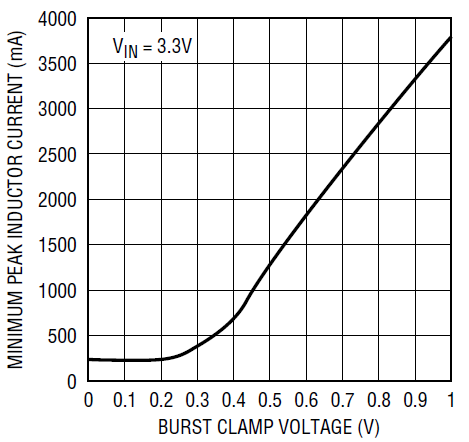
In the LTC3412, the burst clamp level is adjusted by varying the DC voltage at the Sync/Mode pin within a 0V–1V range. The voltage level at this pin sets the minimum peak inductor current during each switching cycle in Burst Mode operation. If the minimum peak inductor current delivers more energy than is demanded by the load current, the internal power switches operate intermittently to maintain regulation.
Figure 1 shows the relationship in Burst Mode operation between the minimum peak inductor current during each switching cycle, and the voltage at the Sync/Mode pin. If the minimum peak inductor current is increased, more energy is delivered to the load during each switching cycle. This forces the control loop to skip more cycles, thus lowering the burst frequency required to maintain regulation. This yields greater efficiency, but also slightly increases output ripple. Conversely, lowering the minimum peak inductor current results in less energy delivered to the load during each switching cycle. This forces the control loop to skip fewer cycles, thus increasing the burst frequency, and reducing the output voltage ripple.

Figure 1. Minimum peak inductor current vs burst clamp voltage
Burst Mode operation provides an efficient solution for light-load applications, but sometimes noise suppression takes priority over efficiency. To reduce noise and RF interference, the LTC3412 can be configured for Forced Continuous operation. In this mode, a constant switching frequency is maintained regardless of the output load. This is important for noise sensitive applications in which it is necessary to avoid switching harmonics in a particular signal band. During dropout, the internal P-channel power MOSFET is turned on continuously to extend the useful operating voltage over the life of the battery. As the battery voltage decreases toward the output voltage, the duty cycle and the on-time increase. Further reduction in the battery voltage forces the P-channel power MOSFET to remain on for more than one cycle, that is, raise the duty cycle to 100%.
A High Efficiency 2.5V/2.5A Step-Down Regulator with All Ceramic Capacitors
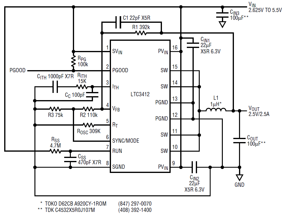
Figure 2 shows a 2.5V step-down DC/DC converter using all ceramic capacitors. This circuit provides a regulated 2.5V output at up to 2.5A from a 2.625V to 5.5V input. Efficiency for this circuit is as high as 95% for a 3.3V input, as shown in Figure 3.

Figure 2. 2.5V, 2.5A regulator using all ceramic capacitors

Figure 3. Efficiency vs load current
Ceramic capacitors offer low cost and low ESR, but many switching regulators have difficulty operating with them. The LTC3412, however, includes OPTI-LOOP compensation, which allows it to operate properly with ceramic input and output capacitors.
The problem many switching regulators have when using ceramic capacitors is that their ESR is too low, which leads to loop instability. That is, the phase margin of the control loop can drop to inadequate levels without the aid of the zero that is normally generated from the higher ESR of tantalum capacitors. The LTC3412 allows loop stability to be achieved over a wide range of loads and output capacitors with proper selection of the compensation components on the ITH pin.
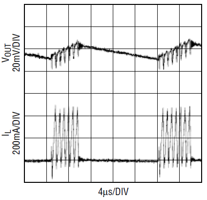
The switching frequency for this circuit is set at 1MHz by a single external resistor, ROSC. Operating at frequencies this high allows the use of a lower valued (and physically smaller) inductor and output capacitor. In this particular application, Burst Mode operation maintains the high efficiency at light loads. During Burst Mode operation, switching cycles are skipped during light loads to reduce switching losses. Efficiency is further improved by powering down the majority of the internal circuitry during the intervals between switching cycles. The Burst Mode operation current is set by the R2 and R3 voltage divider, which generates a 0.32V reference at the Sync/Mode pin. This corresponds to approximately 450mA minimum peak inductor current, as shown in Figure 1. Figure 4 illustrates how Burst Mode operation produces a burst of inductor current pulses that are repeated periodically. Each inductor current pulse increases to approximately 450mA during each switching period before the main power MOSFET is shut off. The process repeats for a multiple number of switching cycles until the change on the output capacitor is refreshed. Once this is accomplished, both the main and synchronous power MOSFETs are held off while the load current is solely supplied by the charge on the output capacitor. This sleep state continues until the output voltage drops low enough to initiate another burst cycle. Varying the voltage on the Sync/Mode pin affects the amplitude of the group of current bursts as well as the frequency at which they are repeated.

Figure 4. Burst Mode operation
Conclusion
The LTC3412 is a monolithic, synchronous step-down DC/DC converter that is well suited for applications requiring up to 2.5A of output current. Its high switching frequency and internal low RDS(ON) power switches make the LTC3412 an excellent choice for compact, high efficiency power supplies.


