36V Dual 1.4A Monolithic Step-Down Converter has Start-Up Tracking and Sequencing
36V Dual 1.4A Monolithic Step-Down Converter has Start-Up Tracking and Sequencing
2007年03月01日
Introduction
The latest DSPs and microcontrollers found in automotive electronics, industrial supplies, and even wall-transformers typically require power supplies with output voltages of both 1.8V and 3.3V and output current capability of 1A or greater. DSL and cable modems also require multiple supplies, usually a combination of a single 5V supply rail and either a 3.3V or 1.8V rail. PCI Express and motherboard interconnect devices supply 3.3V or 5V in addition to a 12V intermediary source. In all of these cases, the supplies must follow a specific start-up sequence or track each other to avoid system latch up or worse.
One common challenge in these applications is producing well-regulated outputs from wide ranging inputs. For instance, a 12V automotive battery produces a voltage range from a low of 4V to a high of 36V. 24V industrial supplies and rectified 12V wall transformers produce similarly wide voltage ranges.

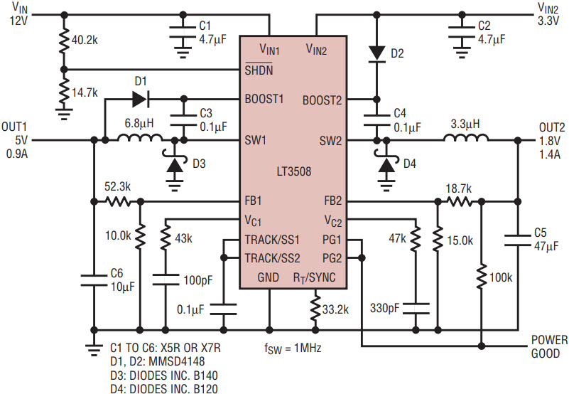
Figure 1. Dual 1.4A monolithic step-down converter with 3.3V and 5V outputs.
The LT3508 simplifies the design of dual output, wide-input-range power converters—especially those that require power supply tracking and sequencing. It is a dual output current mode PWM step-down DC/DC converter with internal power switches capable of generating a pair of 1.4A outputs. Its wide 3.6V to 36V input range makes it suitable for regulating power from a wide variety of sources, including automotive batteries, 24V industrial supplies and unregulated wall adaptors. Both converters are synchronized to a single oscillator programmable from 250kHz up to 2.5MHz and run with opposite phases, reducing input ripple current. The high operating frequency allows the use of small, low cost inductors and ceramic capacitors, resulting in low, predictable output ripple. Each regulator has independent tracking and soft-start circuits and generates a power good signal when its output is in regulation, making power supply sequencing and interfacing with microcontrollers and DSPs easy.

Figure 2. Efficiency for circuit of Figure 1.
Cycle-by-cycle current limit, frequency foldback and thermal shutdown provide protection against shorted outputs, and soft-start eliminates input current surge during start-up. The low current (<2µA) shutdown mode enables easy power management in battery-powered systems.
Versatility Comes from Independent Control of Two 1.4A Channels
Each channel has its own power good, track/soft-start and, unlike most dual channel converters, each has its own VIN pin (more about this below). The boost pin for each channel can be tied to the higher of the two outputs, one to each output (if the channels are turned on and off separately), the input, or an external source. The boost pin voltage must be at least 3V above the switch pin voltage for saturation of the internal power switch.


Figure 3. Dual step-down 5V (a) and 3.3V (b) output voltage transient response.
Individual track/soft-start and power good pins offer a variety of supply tracking and sequencing options. The channels can track each other coincidentally or ratiometrically. The power good pins can be used for sequencing the two channels or simply interfacing with an external microcontroller.

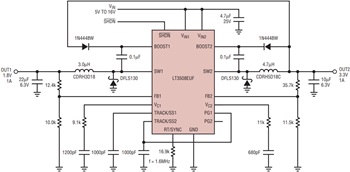
Figure 4. Small dual step-down 1.8V and 3.3V schematic with output sequencing.

Figure 5. Dual step-down 1.8V and 3.3V start-up with output sequencing.

Figure 6. 2.2MHz 28V to 1.8V step-down with cascaded channels and output sequencing.

Figure 7. 2.2MHz 28V to 1.8V step-down start-up with output sequencing.
The unique, separate VIN pins for each channel offer uncommon design flexibility. For instance, the converter can satisfy high VIN/VOUT ratio applications that might be otherwise limited by a single converter’s typical minimum duty cycle constraints. Simply cascade the two converters by attaching the output of one channel to the input of the other channel. This allows the input voltage to be twice as high for a given output voltage and switching frequency without violating minimum duty cycle constraints. In some cases, the separate VIN pins also allow the two channels to be run from two separate current-limited sources that may not have enough power alone to provide full power to both channels’ outputs.
The LT3508’s two channels run 180° out of phase to minimize input current ripple and voltage ripple, thus limiting EMI and reducing the required size of the input capacitor.
High VIN, Low VOUT and Adjustable Switching Frequency
The wide input range of 3.6V to 36V makes the LT3508 suitable for regulating power from a wide variety of sources, including automotive batteries, 24V industrial supplies and unregulated wall adaptors. The operating frequency for the converters can be programmed by a single resistor or synchronized to an external clock ranging from 250kHz to 2.5MHz. High operating frequency allows the use of small, low cost inductors and ceramic capacitors, resulting in low, predictable output ripple. However, selecting a low operating frequency makes it possible to produce high input voltage, low output voltage applications by reducing the duty cycle. The LT3508’s low minimum switch on time of 130ns offers the benefits of high frequency even in high input-output ratio applications. For instance, a frequency of 700kHz is low enough to provide 6V to 36V input voltage range for both 5V and 3.3V outputs at full 1.4A load current (see Figure 1).
The output voltage for the LT3508 can be set as low as the 0.8V reference voltage. With 130ns minimum on-time, the maximum input voltage is calculated by:

VF is the forward voltage of the catch diode, VSW is the internal switch saturation voltage, and fOSC is the oscillator frequency. For 36VIN to 3.3VOUT, fOSC must be below 790kHz. To achieve 36VIN to 1.8VOUT, fOSC must be 470kHz or less. Likewise, a simple 12V to 3.3V step-down ratio is possible with a switching frequency of 2.3MHz. An application converting 12VIN to 5VOUT and 3.3VOUT can take advantage of a high switching frequency of 2.2MHz and remain above the AM band for automotive electronics.
In cases where both a high switching frequency and a high step down ratio are required (as in the case of an automotive power supply that requires a 2.2MHz switching frequency to keep interference outside of the AM band), a cascaded solution can be used. As shown in Figure 6, 28VIN to 1.8VIN is possible if one output is set for 7.7V and tied to the VIN pin of the 1.8V channel. Higher switching frequency reduces inductor and capacitor sizes and achieves faster transient response.
Fast Transient Response
The current mode architecture of the LT3508 control loop yields fast transient response with small, ceramic output capacitors and simple compensation. Small 0805 and 1206 case size 10µF and 22µF 6.3V ceramic output capacitors are typical for up to 1.4A output applications. High temperature coefficient capacitors such as X5R and X7R ceramics are recommended for most designs.
Figure 3 shows the transient response for a typical LT3508 application. Transient response ripple is about 200mVP–P for both the 3.3V output and the 5V output. The response time is about 20µs to 40µs, excellent for 1.4A outputs. This is an important feature when the power supply is used with DSPs and microcontrollers that are sensitive to voltage ripple.

Figure 8. PCI Express power supply with separate inputs.
Low Dropout
The LT3508 features low dropout for output voltages above 3V. The minimum operating voltage of the device is determined either by the LT3508’s undervoltage lockout or by its maximum duty cycle. If VIN1 and VIN2 are tied together, the undervoltage lockout is at 3.7V or below. If the two inputs are used separately, then VIN1 has an undervoltage lockout of 3.7V or below and VIN2 has an undervoltage lockout of 3V or below. Because the internal supply runs off VIN1, channel 2 will not operate unless VIN1 is above its undervoltage lockout. The dropout of the 5VOUT circuit shown in Figure 1 is less than 1V, with start-up occurring at a minimum of 5.9V and the converter running down to 5.5V before dropout occurs.
Unlike many fixed frequency regulators, the LT3508 can extend its duty cycle by turning on for multiple cycles. The LT3508 will not switch off at the end of each clock cycle if there is sufficient voltage on the boost capacitor. Eventually, the voltage on the boost capacitor falls and requires refreshing. A bigger boost capacitor allows for higher maximum duty cycle. Circuitry detects a depleted boost capacitor and forces the switch to turn off, allowing the inductor current to charge up the boost capacitor. This places a limitation on the maximum duty cycle. The minimum input voltage can be calculated as:

βSW is the switch current to boost current ratio. Refer to the data sheet section “Minimum Operating Voltage” for details.
Track/Soft-Start and Power Good Pins Simplify Supply Sequencing
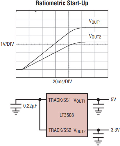
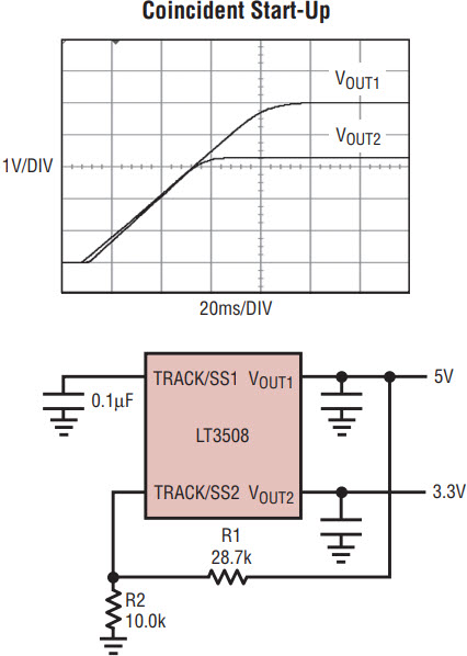
DSPs and microcontrollers require power supply sequencing and tracking. Both LT3508 channels have independent tracking and soft-start circuits and each generates a power good signal when its output is in regulation. Most start-up/shut-down scenarios are possible by combining the function of the track/soft-start (TRACK/SS) with the power good (PG) pins. Figure 9 shows how easy it is to implement independent channel soft-start, ratiometric start-up, coincident start-up, output sequencing, and externally controlled power up and power down.


Figure 9. Tracking and soft-start options.
Soft-start prevents inrush current spikes, which can drag down the source voltage upon start-up and cause other system problems. Simple soft-start of each channel requires only a capacitor on the pin (Figure 9a). The rate of soft-start is determined by the size of capacitor and by the capabilities of the power source.
As the name suggests, the TRACK/SS pins also facilitate supply tracking, including ratiometric, coincident and externally controlled start-up and shut-down. Figure 9d shows how to connect the PG pin of one channel to the track pin of another channel to sequence the two—one channel is held off until the other channel is good.
The track/soft-start function can also be used to power a channel down, but to minimize current draw, shut down the regulator via the shutdown (SHDN) pin as described below.
Low Shutdown Current
When the shutdown pin is pulled low, both channels turn off and the part consumes a very low quiescent current (<2µA), saving battery energy and extending lifetime. The shutdown pin can also be used as a 2.63V accurate undervoltage lockout (UVLO) with a resistor divider from VIN. In shutdown, the power good comparator is disabled and not valid and the soft-start capacitors are reset.
TSSOP-16 and QFN Packages
The LT3508 is available in two types of thermally-enhanced packages. The UF package is a 4mm × 4mm 24-pin QFN. The FE package is a 16-pin thermally-enhanced TSSOP surface mount with an exposed thermal pad. Both packages have equally low 40°C/W junction-to-ambient thermal impedance and 10°C/W junction-to-case impedance, important for applications that require a high input voltage, high switching frequency and high load current, all of which raise the junction temperature.
Conclusion
The LT3508 is a wide input voltage 36V dual 1.4A monolithic step-down converter with tracking/soft-start pins and power good pins for power supply sequencing and simple diagnostic interface with DSPs and microcontrollers. It has adjustable switching frequency from 250kHz to 2.5MHz, either set by a resistor or synchronized to an external source. Its thermally enhanced packages and E and I-grade temperature ratings allow it to be used in thermally demanding environments. Separate VIN pins for each channel provide the capability of cascading channels and achieving extreme VIN to VOUT ratios by using the output of one channel as the input for the other.
著者について
Keith Szolushaは、アナログ・デバイセズ(カリフォルニア州サンノゼ)のアプリケーション・ディレクタです。2000年からIPSパワー製品グループに所属しています。主に降圧/昇圧/昇降圧コンバータ、LEDやGaNに対応するコントローラ/ドライバなどの製品を担当。また、電源製品向けのEMIチャンバの管理も担っています。マサチューセッツ工科大学で1997年に電気工学の学士号、1998年に同修士号を取得。テクニカル・ライティングの集中コー...


