
MAXREFDES1273


製品概要
設計リソース
説明
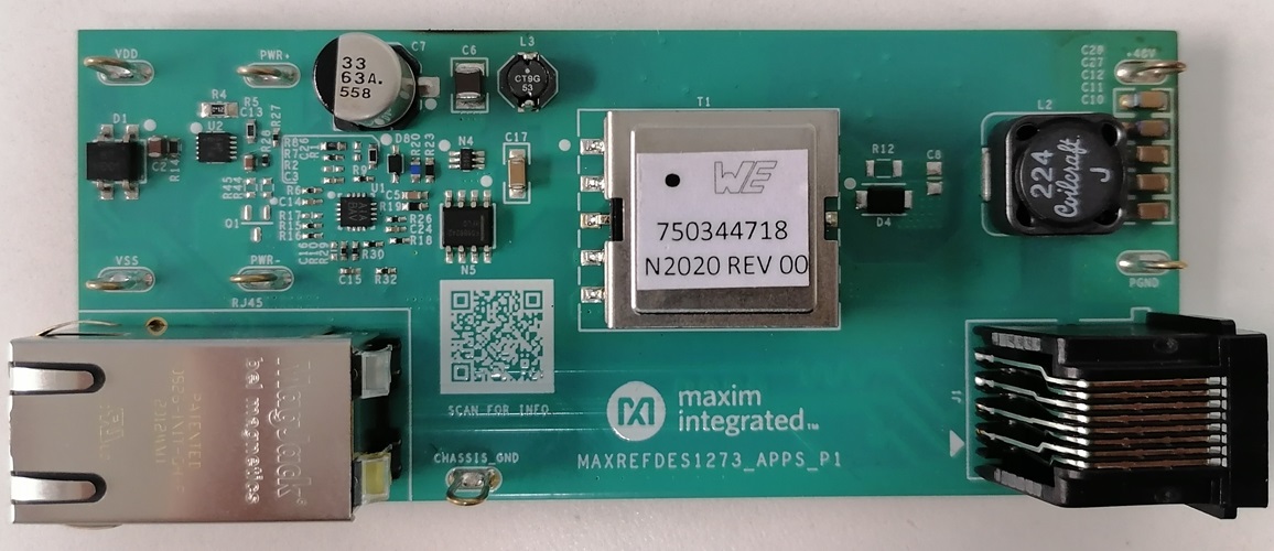
The MAXREFDES1273 is a Power-over-Ethernet (PoE) powered device (PD) and an active clamp forward DC-DC converter (ACFC) that delivers up to 850mA at 48V from 39V to 57V supply voltage. It is designed for the PD system to comply with the IEEE® 802.3af/at standard in a PoE system. The MAXREFDES1273 illustrates techniques using the active clamp forward topology to generate isolated output. This document explains how the MAX5969B and MAX5974C can be used to design the PD to generate 48V from 39V to 57V input voltage. An overview of the design specification is shown in table below.
Power over Ethernet is a technology that allows network cables to deliver power to a PD through power sourcing equipment (PSE) or midspan and has many advantages over traditional methods of delivering power. The PoE technology allows power and data to be combined, removing the need for altering the AC mains infrastructure and can be installed by nonelectricians. Power over Ethernet is an intelligent system designed with protection at the forefront, preventing overload, underpowering, and installation errors, while allowing simple scalability and reliability.
The MAX5974C provides control for wide-input-voltage, active-clamped, current-mode pulse-width modulation (PWM), forward converters in PoE powered device applications. The MAX5974C is well-suited for universal or telecom input range.
機能と利点
- Programmable switching frequency from 100kHz to 600kHz
- Programmable frequency dithering for low-EMI, spread-spectrum operation
- Programmable dead time, PWM soft-start, current slope compensation
- Programmable feed-forward maximum duty-cycle clamp, 80% maximum limit
- Frequency foldback for high-efficiency light-load operation
- Internal bootstrap UVLO with large hysteresis
- 100μA (typ) startup supply current
- Fast cycle-by-cycle peak current-limit, 35ns typical propagation delay
- 115ns current-sense internal leading-edge blanking
- Output short-circuit protection with hiccup mode
- Reverse current limit to prevent transformer saturation due to reverse current
詳細
The MAXREFDES1273 is a Power-over-Ethernet (PoE) powered device (PD) and an active clamp forward DC-DC converter (ACFC) that delivers up to 850mA at 48V from 39V to 57V supply voltage. It is designed for the PD system to comply with the IEEE® 802.3af/at standard in a PoE system. The MAXREFDES1273 illustrates techniques using the active clamp forward topology to generate isolated output. This document explains how the MAX5969B and MAX5974C can be used to design the PD to generate 48V from 39V to 57V input voltage. An overview of the design specification is shown in Table 1.
| Parameter | Symbol | Min | TYP | Max |
| Input Voltage | VIN | 39V | 48V | 57V |
| Frequency | fSW | 250kHz | ||
| Maximum Efficiency | η | 88% | ||
| Output Voltage | VOUT | 47.52V | 48V | 48.48V |
| Output Voltage Ripple | ΔVOUT | 480mV | ||
| Output Current Range | IOUT | 0A | 850mA | |
| Output Power | POUT | 0W | 40.8W | |
Power over Ethernet is a technology that allows network cables to deliver power to a PD through power sourcing equipment (PSE) or midspan and has many advantages over traditional methods of delivering power. The PoE technology allows power and data to be combined, removing the need for altering the AC mains infrastructure and can be installed by nonelectricians. Power over Ethernet is an intelligent system designed with protection at the forefront, preventing overload, underpowering, and installation errors, while allowing simple scalability and reliability.
The MAX5974C provides control for wide-input-voltage, active-clamped, current-mode pulse-width modulation (PWM), forward converters in PoE powered device applications. The MAX5974C is well-suited for universal or telecom input range.
Other features include the following:
- Programmable switching frequency from 100kHz to 600kHz
- Programmable frequency dithering for low-EMI, spread-spectrum operation
- Programmable dead time, PWM soft-start, current slope compensation
- Programmable feed-forward maximum duty-cycle clamp, 80% maximum limit
- Frequency foldback for high-efficiency light-load operation
- Internal bootstrap UVLO with large hysteresis
- 100µA (typ) startup supply current
- Fast cycle-by-cycle peak current-limit, 35ns typical propagation delay
- 115ns current-sense internal leading-edge blanking
- Output short-circuit protection with hiccup mode
- Reverse current limit to prevent transformer saturation due to reverse current
This reference circuit consists of the MAX5969B PD controller and an isolated active forward DC-DC converter using the MAX5974C to demonstrate a 48V DC output application. A 1GbE RJ45 magnetic jack is also included along with two diode bridges for separating data and DC power provided by an endspan or midspan PoE system. The power supply delivers up to 1A at 24V. Table 1 is an overview of the design specifications.
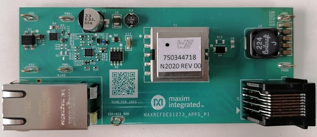
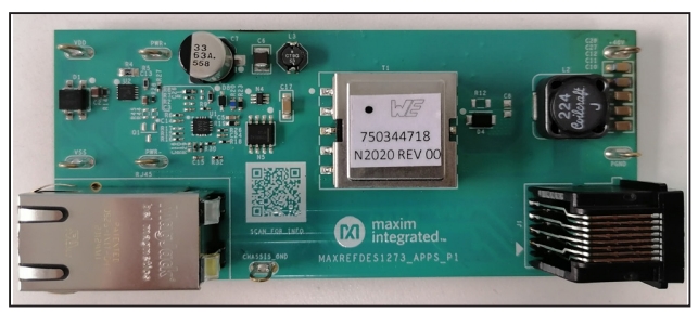
This document describes the hardware shown in Figure 1. It provides a detailed technical guide to designing a complete interface for a PD to comply with the IEEE 802.3af/at standard in a PoE, class 4 system and an isolated ACFC using Analog Devices's MAX5974C controller. The power supply has been built and tested.
A PoE system delivers power and data to an end device (PD) typically through an RJ45 cable power from an endspan (Power Sourcing Equipment [PSE]) (see Figure 2) or a midspan (see Figure 3). The power is separated from the data through diode bridges to deliver a typical 48 V for efficient power transfer, which is low enough to be considered a safe voltage, and this removes the need to rewire AC mains, and saves cost.
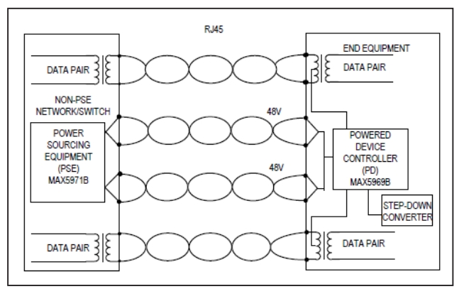
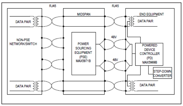
Although this voltage is safe for humans, it still can damage equipment if not properly delivered. This is where MAX5969B classification is required, ensuring the equipment can handle the power delivery. Before the PSE can enable power to a connected Internet protocol (IP) camera or other PD, it must perform a signature detection.
Signature Detection
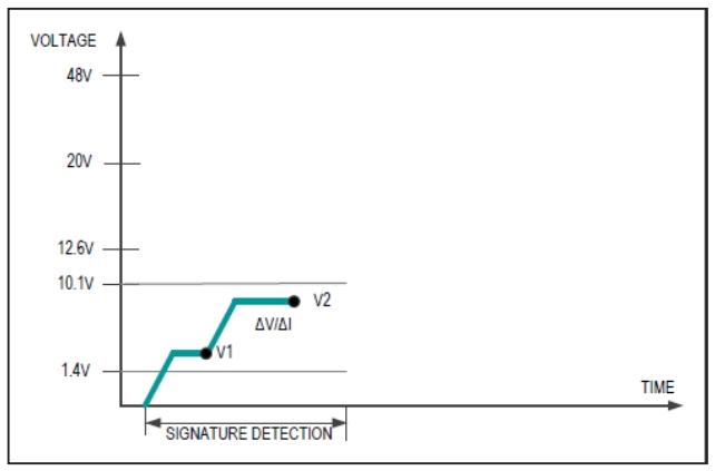
Signature detection uses a lower voltage to detect a characteristic signature of IEEE-compatible PDs (with a 24.9kΩ resistance). See Figure 4. Once this signature is detected, the PSE knows that higher voltages can be safely applied. The PSE applies two voltages on VIN in the range of 1.4V to 10.1V (1V step minimum) and then records the current measurements at the two applied voltages. The PSE then computes the change in current when each voltage is applied (ΔV/ΔI) to ensure the presence of the 24.9kΩ signature resistor.
Classification
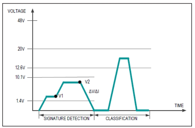
In classification mode, the PSE classifies the PD based on the power consumption required. (The IEEE 802.3af/at standard defines only Class 0 to 4 and Class 5 for any special requirement.)
An external resistor (RCLS) of 30.9Ω connected from CLS to VSS sets the classification current. The PSE determines the class of a PD by applying a voltage at the PD input and measuring the current sourced from the PSE. When the PSE applies a voltage between 12.6V and 20V, the MAX5969A/MAX5969B exhibit a current of 36mA to 44mA.
The PSE uses the classification current information to classify the power requirement of the PD (MAX5969B).
The classification current includes the current drawn by RCLS and the supply current of the MAX5969A/MAX5969B so the total current drawn by the PD is within the IEEE 802.3af/at standard figures. The classification current is turned off whenever the device is in power mode (see Figure 5).
Power Mode
The final stage after detection and classification of a newly connected PD is to enable power. The 48V supply from the PSE is connected to the PD through the RJ45 cable. Once enabled, the PSE continues to monitor how much current is being delivered to the PD and cuts power to the cable if the power drawn is not within the correct range. This protects the PSE against overload, underpowering and ensuring that the PSE is disconnected from the cable if the PD is unplugged or faulted. See Figure 6.
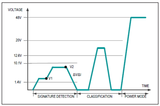
The MAX5969B enters power mode when VIN rises above the undervoltage lockout (UVLO) threshold (VON). Note that VON/VOFF = 38.6V/31V for the MAX5969B. When VIN rises above VON, the MAX5969B turns on the internal n-channel isolation metal-oxide semiconductor field-effect transistor (MOSFET) to connect GND to RTN. The open-drain power-good (PG) output remains low for a minimum of tDELAY until the power MOSFET fully turns on to keep the downstream DC-DC converter disabled during inrush. The open-drain PG output is also connected to three small-signal transistors to prevent the DC converters from powering up before the power from the PD is allowed.
| Class | Maximum Power Used by PD (W) | RCLS (Ω) | VIN* (V) | Class Current Seen at VIN (mA) | IEEE 802.3af/at PSE Classification Current Specifications (mA) | ||
| Min | Max | Min | Max | ||||
| 0 | 0.44 to 12.95 | 619 | 12.6 to 20 | 0 | 4 | 0 | 5 |
| 1 | 0.44 to 3.94 | 117 | 12.6 to 20 | 9 | 12 | 8 | 13 |
| 2 | 3.84 to 6.49 | 66.5 | 12.6 to 20 | 17 | 20 | 16 | 21 |
| 3 | 6.49 to 12.95 | 43.7 | 12.6 to 20 | 26 | 30 | 25 | 31 |
| 4 | 12.95 to 25.5 | 30.9 | 12.6 to 20 | 36 | 44 | 35 | 45 |
| 5 | > 25.5 | 21.3 | 12.6 to 20 | 52 | 64 | ||
Place the input capacitor, classification resistor, and transient voltage suppressor as close as possible to the MAX5969A/MAX5969B. Use large surface-mount technology (SMT) component pads for power dissipating devices such as the MAX5969A/MAX5969B and the external diodes. Use short and wide traces for high-power paths.
The MAX5969B enters UVLO when the input voltage drops below 31V. When the input drops below this value, the isolation MOSFET switches off, disconnecting the 48V from the buck converters. The MAX5969B exits UVLO when the input exceeds 38.6V, where the isolation MOSFET switches on again, connecting the MAX5974C forward converter.
The single ended forward converter has always been a favorite of designers for single and multiple output power supplies in the range from watts to kilowatts. In this topology, a second out-of-phase winding (reset winding) is used to reset the magnetic flux in the power transformers core during the time the secondary side freewheeling diode is conducting. If the number of turns on this winding is equal to the number of turns on the main transformers' primary winding the drain-source voltage of the main power switch is limited (excluding ringing due to leakage inductance and parasitic capacitance in the circuit) to two times the input voltage of the power supply but so too is the maximum duty cycle limited to less than 50%. This duty cycle limit can be extended above 50% to improve transformer utilization by increasing the number of turns on the reset winding but only at the expense of a higher drain-source voltage (increased voltage stress and switching power losses) on the main power switch.
These and other limitations of the forward converter can easily be overcome when the designer fully understands the operation and unique benefits of the ACFC topology.
The main components of an ACFC are shown in Figure 7. The active clamp consists of a P-channel MOSFET (QAUX) and a clamp capacitor (CCLAMP). The difference between the traditional forward converter and the ACFC occurs when the main power MOSFET (QMAIN) is off. The reset winding and diode of the traditional forward converter clamps the drain-source voltage of QMAIN to approximately twice the power supply input voltage during the first half of the interval when QMAIN is off whereas in the ACFC the drain-source voltage of QMAIN is clamped to an intermediate voltage between VIN and 2VIN for the full interval when QMAIN is off.
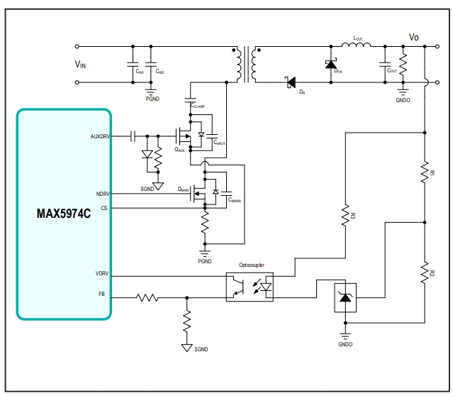
The benefits of the ACFC topology go far beyond reducing the voltage stress on the main power MOSFET and increasing the duty cycle limit. Further benefits provided by the ACFC topology are as follows:
- Zero voltage switching (ZVS) can be achieved for QMAIN and QAUX over the full load range by careful design thus significantly improving power supply efficiency.
- A smaller output inductance can be used due to higher operating duty cycle.
- Operating at higher than 50% duty cycle allows a higher secondary to primary turns ratio on the transformer leading to a lower reflected current from secondary to primary and thus a lower peak current in the main power MOSFET.
- There is lower electromagnetic interference (EMI) due to the ZVS nature of the switching.
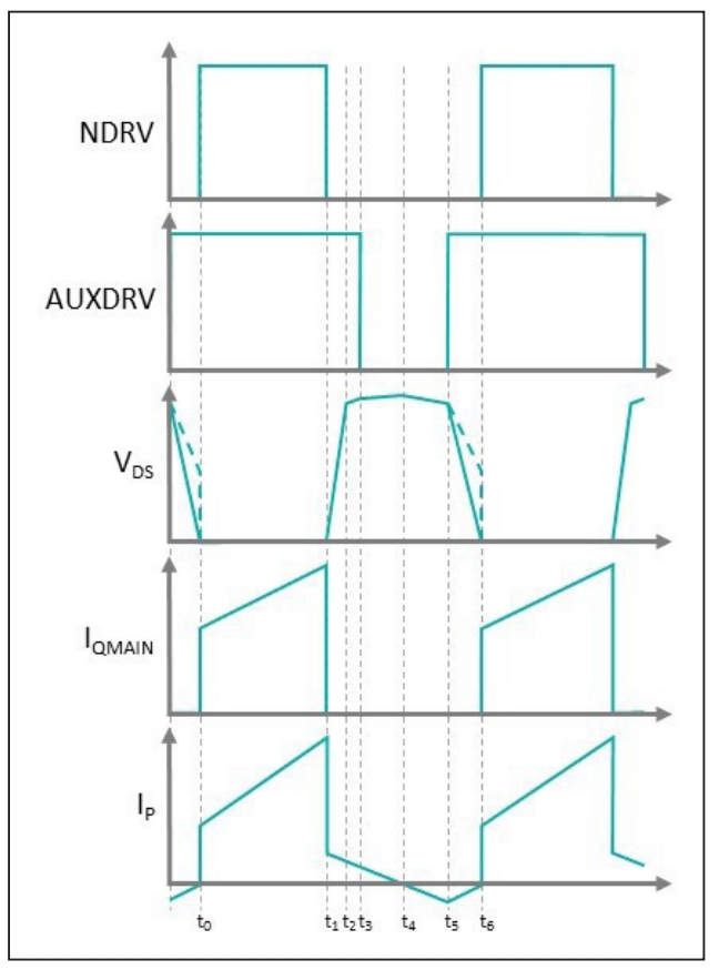
- Figure 8 shows the main steady state waveforms of the ACFC. It is very important to understand what is happening during one complete switching cycle of the converter.
Time Interval t0 to t1
QMAIN turns on at t0 QAUX remains off. The primary current IP, which is the sum of the transformer magnetizing IMAG and the reflected secondary current ISEN, flows through the primary of the transformer and QMAIN. IP ramps up linearly while QMAIN is on. Current also flows on the secondary side through the rectifying diode DR while QMAIN is on. No current flows through QAUX during this interval.
Time Interval t1 to t2
QMAIN turns on at t1. DR is now reverse biased so the reflected secondary current component of IP is zero. IP is now only the transformer magnetizing current. It decreases toward zero charging the drain capacitance of QMAIN, CdMAIN.
Time Interval t2 to t3
At t2, the drain voltage of QMAIN reaches the same voltage level as the voltage across CCLAMP, the body diode of QAUX becomes forward biased, and the voltage across CCLAMP increases. The rate of increase of the drain voltage of QMAIN is now much lower since CCLAMP >> CdMAIN.
Time Interval t3 to t4
At t3, QAUX turns on. QAUX switches under the ZVS condition providing it turns on after its body diode starts conducting (at t2) and before IP goes negative (at t4). QAUX must turn on before t4 otherwise IP has no path to go negative at t4.
Time Interval t4 to t5
At t4, IP is now negative and is discharging CCLAMP through QAUX, which is on. IP continues to become more negative and the drain voltage of QMAIN decreases.
Time Interval t5 to t6
QAUX turns off at t5 and the voltage across CCLAMP stops decreasing. The only current path now available for the negative IP to flow is out of CdMAIN. The voltage across CdMAIN keeps decreasing until IP reaches zero. VDS decays to zero by t6 providing the energy stored in the magnetizing and leakage inductance at t5 is greater than the energy stored in CdMAIN at t5. ZVS occurs if this condition is met otherwise QMAIN switches on at t6 at some intermediate voltage between zero and VDSMAX.
Design Procedure for the ACFC
Now that the principle of operation of the ACFC is understood, a practical design example can be illustrated. The converter design process can be divided into several stages: power stage design, setup of the MAX5974C ACFC current mode controller, and the feedback loop. This document is primarily concerned with the power stage design, and the feedback loop is intended to complement the information contained in the MAX5974C data sheet for details on how to set up supervisory and protection functions of the controller.
The following design parameters are used throughout:
| Parameter | Value |
| VIN | Input Voltage |
| VOUT | Output Voltage |
| ΔVOUT | Output Ripple Voltage |
| IOUT | Output Current |
| POUT | Output Power |
| η | Target Maximum Efficiency |
| PIN | Input Power |
| fSW | Switching Frequency |
| D | Duty Cycle |
| n | Primary-Secondary Turns Ratio |
| NP | Turns of Primary Winding |
| NS | Turns of Secondary Winding |
| NAUX | Turns of Tertiary Winding |
The above symbols are sometimes followed by parentheses to indicate whether minimum or maximum values of the parameters are intended; for example, minimum input voltage is intended by the symbol VIN(MIN). Otherwise, typical values are intended.
In addition, through the design, procedure reference is made to the schematic in another document.
Step 1: Choosing a Suitable Switching Frequency
The MAX5974C can operate at a switching frequency between 100kHz and 600kHz. A lower switching frequency optimizes the design for efficiency, whereas a higher frequency allows for smaller inductive and capacitive components as well as lower costs. A switching frequency of 250kHz was chosen for this design. R15 sets the switching frequency according to the following expression:
Step 2: Setting the Maximum Duty Cycle
One advantage of using the MAX5974C for the ACFC is the maximum allowable duty cycle. If the duty cycle is not clamped at some maximum value, transformer saturation can occur, resulting in catastrophic failure, and QMAIN can be subjected to increased voltage stress. A maximum duty cycle of 80% is recommended at switching frequencies up to 400kHz. An initial choice of 62% allows for some design margin.
Step 3: Calculating the Transformer Turns Ratio
For the forward converter topology, the transformer turns ratio is given by the following expression:
where VMDS(ON) is the drain-source voltage of QMAIN in the on state, VDR(F) is the forward voltage drop of DR, and VLOUT is the resistive DC voltage drop across the output inductor winding. DMAX occurs at VIN(MIN). Assuming VMDS(ON) = 0.2 V, VDR(F) = 0.5 V, and VLOUT = 0.2 V, then
Step 4: Calculating Turns of Primary Winding NP, Secondary Winding NS, and Tertiary Winding NAUX
For the forward converter topology, the transformer turns of the primary winding is given by the following expression:
where ΔB is the flux density deviation of the transformer, which should be below or equal to 2000 GS, Ae is the effective magnetic cross-section of the transformer core. Considering the maximum output power and the size of this design, we chose EFD20 as the transformer core. If the effective magnetic cross of EFD20 is 0.31 cm², then
We use 16 turns for the primary winding; for the secondary turns,
If we use 32 turns for the secondary winding, then
During normal operation, the voltage at IN is normally derived from a tertiary winding of the transformer. For the tertiary winding turns,
We use 8 turns for the tertiary winding.
Step 5: Calculate D at VIN(MIN), VIN(TYP), and VIN(MAX)
Re-arranging the expression in Step 3 gives
And,
| DMIN | DTYP | DMAX |
| 0.425 | 0.5058 | 0.624 |
Step 6: Calculate VMDS(MAX) of QMAIN at DMIN, DTYP, and DMAX
For the forward converter topology, VMDS is given by the following expression:
Given the DMAX occurs at VIN(MIN), DTYP occurs at VIN(TYP), and DMIN occurs at VIN(MAX), we have
| VMDS at VIN(MAX) | VMDS at VIN(TYP) | VMDS at VIN(MIN) |
| 99.13V | 97.13V | 103.72V |
The critical operating parameters of the converter are now fixed, so it is possible to continue the design process of calculating and selecting suitable components for the power train.
Step 7: Calculating and Selecting LOUT
The output inductance is calculated assuming a maximum peak-to-peak output ripple (ΔISEC), which occurs at maximum input voltage. The output inductance can be calculated as follows:
Where VDFW(F) is the forward voltage drop of the secondary freewheeling diode and %ΔISEC (0.6, typical) is the ratio of peak-to-peak output inductor current ripple to the average output current at maximum input voltage. We have
Where IOUT = 850mA and VDFW(F) = 0.5V. In this design, we can choose a standard ±20% tolerance 22 μH inductor. Finally, we must choose an output inductor with a DC winding resistance that is sufficiently low to ensure that VLOUT is less than 0.2 V at IO(MAX) because this is the value we have used for VLOUT in the preceding calculations. We should choose an inductor with
The final inductor value chosen for this design is a 10% tolerance 220μH/1.42A/335mΩ inductor MSS1260-224KL from Coilcraft®.
Step 8: Calculate the Transformer Magnetizing Inductance LMAG and the Secondary and Primary Peak Winding Currents, IS(PK) and IP(PK)
The physical design of the power transformer is outside the scope of this document; however, it is necessary to calculate the critical parameters of the transformer.
We must first calculate the minimum output inductor ripple current by rearranging the expression in Step 7 and remembering that minimum ripple occurs at DMAX as follows:
LOUT(MAX) for the selected ±20% 100μH inductor is 120μH. So,
For the MAX5974C ACFC current mode controller to function properly, the maximum magnetizing current referred to the primary side of the transformer must be less than the minimum output inductor ripple current reflected to the primary side of the transformer. So,
And,
To allow for design margin, we chose a value for IMAG = 0.5A (85% of IMAG(MAX)). The next step is to calculate a minimum magnetizing inductance that ensures that IMAG(MAX) < 0.5A. The following expression is used to calculate LMAG(MIN):
So,
Allowing for a ±30% tolerance for the magnetizing inductance, we can choose LMAG = 300μH ± 30%.
Figure 9 illustrates the output inductor current IL, the secondary transformer current IS, primary transformer current IP, and the current flowing in main power MOSFET, IQMAIN.
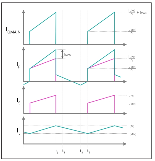
Although IP appears linear when both QMAIN and QAUS are off (t1 to t3 and t5 to t6), there is a resonance between the two end points, which makes ZVS possible.
The peak current in the secondary winding IS(PK) is equal to the peak current in the output inductor IL(PK). The peak current IL(PK) is a maximum at VIN(MAX) and IO(MAX), therefore:
And,
So,
The peak current in the primary winding IP(PK) is the peak current in the secondary winding reflected back to the primary side of the transformer plus IMAG. Therefore,
So,
The transformer must not saturate at a magnetizing force of (NP × IP(PK)) where NP is the number of turns on the primary winding.
Step 9: Calculate the Maximum RMS Currents in the Transformer Secondary and Primary Windings, IS(RMS) and IP(RMS)
The maximum root mean square (RMS) currents in the transformer primary and secondary windings occur at VIN(MIN) and IOUT(MAX), i.e., at DMAX. To calculate IS(PK) at VIN(MIN), we must first calculate IL(PK) in the output inductor at VIN(MIN).
Following the process of Step 8 we have, at VIN(MIN),
And,
So,
The current at which the secondary rectifying diode DR starts to conduct IS(V), corresponds to IL(MIN). So,
We can now calculate the maximum RMS current in the secondary winding as follows:
So,
Referring to Figure 8, we can calculate the instantaneous current in QMAIN at turn-on and turn-off, IQM(t-on) and IQM(t-off), respectively.
The maximum RMS current in QMAIN can now be calculated as follows:
The transformer primary current IP, as shown in Figure 9, is a more complex waveform than IQM. IP is a superposition of IQM and IQA, and the resonant currents that flow during the time intervals when both QMAIN and QAUX are off. Nevertheless, it is reasonable to use the approximation that
We now have all the critical parameters of the transformer, as detailed in the following table.
| Parameter | Symbol | Value |
| Primary Magnetizing Inductance | LMAG | 300 μH ± 30% |
| Primary Peak Current | IP(PK) | 2.76A |
| Primary RMS Current | IP(RMS) | 1.65A |
| Turns Ratio (NP/NS) | n | 0.5 |
| Primary Turns | NP | 16T |
| Secondary Turns | NS | 32T |
| Tertiary Turns | NAUX | 8T |
| Secondary Peak Current | IS(PK) | 1.13A |
| Secondary RMS Current | IS(RMS) | 0.534A |
Using these parameters in the table, a suitable transformer can be designed.
Step 10: Choose a Suitable MOSFET for QMAIN
All the necessary parameters for selecting a suitable QM have already been calculated.
From Step 6,
From Step 8,
And,
Allowing for reasonable design margin, Fairchild part number FDC86242 was chosen for this design with the following specifications:
| Maximum D-S Voltage | 150V |
| Continuous Drain Current | 3.3A |
| D-S Resistance at VGS = 4.5 V | 98mΩ |
| Total Gate Charge Qg | 13nC |
Step 11: Choose Suitable Rectifying and Freewheeling Diode for DR and DFW, Respectively
Almost all the necessary parameters for selecting a suitable DR have already been calculated. In Step 8, we calculated IS(PK), the same peak current that flows in DR. So,
In Step 9, we calculated the maximum RMS current in the transformer secondary winding IS(RMS), the same RMS current that flows in DR.
So,
The peak reverse voltage seen by DR is given by
So,
For the freewheeling diode DFW, we have
The maximum RMS current in the freewheeling diode occurs at VIN(MAX) and is calculated using
where
So,
Finally, the peak reverse voltage seen by DFW is given by
Allowing for a reasonable design margin, a Schottky diode, part number RB068LAM150TF, was selected for both DR and DFW.
Step 12: Choose Suitable P-Channel MOSFET for the Active Clamp Switch QAUX
Only a portion of the primary magnetizing current flows in the drain of the active clamp switch during the interval between t3 and t5. If we assume as the worst case that all the magnetizing current flows in QAUX, then we can estimate the RMS current flowing in the drain of QAUX as follows:
At such a low RMS current, conduction losses are very low, so choosing a MOSFET with a low gate charge should be the primary consideration, with low RDS(ON) being only a secondary concern. In addition to conduction losses being very low, switching losses are also negligible, because the body diode of QAUX is conducting before QA turns on. The repetitive peak current in QAUX is the maximum primary magnetizing current:
The active clamp switch experiences the same voltage stress as the main power switch; referring to Step 6 this is as follows:
Allowing for reasonable design margin, Vishay P-Channel MOSFET, SI1411DH-T1-GE3, was chosen for this design, with the following specifications:
| Maximum D-S Voltage | 150V |
| Peak Repetitive Drain Current | 0.42A |
| D-S Resistance at VGS = 7 V | 2.05Ω |
Step 13: Choose a Suitable Clamp Capacitor C17
The clamp capacitor (C17) helps in resetting the flux in the transformer core as well absorbing leakage inductance energy, and it forms a complex pole-zero pair with the magnetizing inductance (LMAG) of the transformer at a frequency fR.
The value of the clamp capacitor for a 20% voltage ripple is calculated as:
We chose 4.7nF as the clamp capacitor.
The voltage stress on the clamp capacitor can be calculated as:
The C17 should be rated for at least 1.4× the calculated worst-case VC12 stress.
Step 14: Calculate and Choose the Output Capacitor COUT
Output capacitance value can be calculated based on either steady-state voltage ripple or transient voltage ripple. If the design consideration is the transient steady-state voltage ripple, then the output capacitor is usually sized to support a step load of 25% of the rated output current (IOUT) in isolated applications so that the output-voltage deviation is contained to 3% of the rated output voltage. The output capacitance can be calculated as follows:
where COUT is the total capacitance required at the output, ISTEP is the load step, tRESPONSE is the response time of the controller, and ΔVOUT is the allowable output voltage deviation during the load transient.
Response time of the controller tRESPONSE is given as
The complex pole-zero pair frequency formed due to clamp capacitor and magnetizing inductance of the converter is given as
fC is the target closed-loop crossover frequency, which is given as
So, the response time of the controller tRESPONSE is given as
Choose ISTEP equal to 25% of output current, ISTEP = 0.2125A, ΔVOUT = 3% of output voltage, which is equal to 1440 mV.
So, the output capacitance is given as
In this design, to get smaller output voltage ripple, 5 × 2.2μF ceramic capacitors are used. Considering 20% derating of the ceramic capacitors, the total ceramic output capacitance would be 5 × 2.2μF × 0.8 = 8.8μF.
Step 15: Calculate and Choose the Input Capacitor CIN
Capacitor selection is based on switching ripple. The maximum average input current drawn from the input power supply at minimum input voltage can be calculated as
The voltage ripple present on the input capacitor is 2% of the minimum input voltage and is given as
The value of the input ceramic capacitor with the above assumed ripple voltage can be calculated as follows:
In this design, 2 × 1μF ceramic capacitors and one 33μF electrolytic capacitor are used for the input capacitor.
Step 16: Calculating and Selecting the Peak Current Limit Resistors (R21 and R25)
The current-sense resistor (RCS in the Typical Application Circuits), connected between the source of the n-channel MOSFET and PGND, sets the current limit. The current limit comparator has a voltage trip level (VCS-PEAK) of 400 mV. Use the following equation to calculate the value of RCS:
Two standard 100mΩ current-sense resistors are used in the design. Low-inductance current-sense resistors should be used for R21 and R25.
関連資料
-
MAXREFDES1273 Design Files2021/11/21ZIP1 M
サポートおよびトレーニング
技術的なご質問についての回答は、ナレッジベースを検索してください。また、アナログ・デバイセズのアプリケーション・エンジニアの専任チームが、技術的なご質問にお答えいたします。