MAXREFDES1123
80V/5mA, High-Voltage, Compact Boost Power Supply Using MAX1523


製品概要
設計リソース
説明
The MAXREFDES1123 is a compact boost power-supply design for high-voltage applications with low current requirements where extremely low cost and small size are top priorities. This design provides an 80V output and up to 5mA of load current. This power supply is designed specifically to provide a simple application circuit at high voltage and to minimize the size and number of external components, making it ideal for low-cost consumer electronics applications.
This design is centered around the MAX1523 simple SOT23 boost controller. The design is tested at 5V nominal voltage input. The output voltage is within 1% error margin.
機能と利点
- Small Size (134mm2)
- 80V/5mA Output
- Low Quiescent Current (25μA typ)
- Pin-Selectable Maximum Duty Factor
- Internal Soft-Start and Short-Circuit Protection
- Discontinuous Conduction Mode (DCM)
使用されている製品
詳細
The MAXREFDES1123 is a compact boost power-supply design for high-voltage applications with low current requirements where extremely low cost and small size are top priorities. This design provides an 80V output and up to 5mA of load current. This power supply is designed specifically to provide a simple application circuit at high voltage and to minimize the size and number of external components, making it ideal for low-cost consumer electronics applications.
This design is centered around the MAX1523 simple SOT23 boost controller. The design is tested at 5V nominal voltage input. The output voltage is within 1% error margin.
Other features include the following:
- Small Size (134mm2)
- 80V/5mA Output
- Low Quiescent Current (25µA typ)
- Pin-Selectable Maximum Duty Factor
- Internal Soft-Start and Short-Circuit Protection
- Discontinuous Conduction Mode (DCM)
This is a single-output power supply using the MAX1523 compact boost controller. The power supply is designed for a high-voltage application with low-current requirements. This design can deliver up to 5mA at 80V. Table 1 shows an overview of the design specification.
| PARAMETER | SYMBOL | MIN | MAX |
| Input Voltage | VIN | 4.5V | 5.5V |
| Output Voltage | VOUT | 80V | |
| Output Current | IOUT | 0mA | 5.5mA |
| Output Voltage Ripple | VRIPPLE | 226mV | |
| Efficiency | η | 83% |
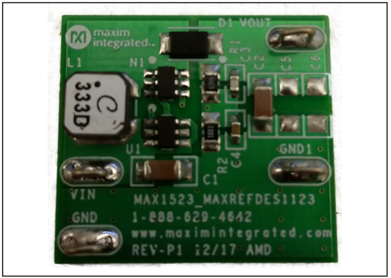
This document describes the hardware shown in Figure 1. It provides a detailed systematic technical guide for designing a boost controller using the MAX1523 for high voltage, low current, and small size. Refer to the MAX1523 IC data sheet for device operation details. The power supply has been built and tested, details of which follow later in this document.
The MAX1523 can be operated in either continuous conduction mode (CCM) or discontinuous conduction mode (DCM). CCM is most commonly used in a switching regulator due to its advantage of lower peak current, reduced output power losses, and reduced output ripple. However, there are two common reasons not to run the switching regulator in CCM:
- High output voltage. In this case, the output-to-input voltage ratio exceeds the level obtainable by
the MAX1523 maximum duty factor. If the number of maximum duty cycle exceeds 80%, then the
MAX1523 must be designed in DCM. Maximum
duty cycle can be calculated using this formula:

where VD is the forward voltage drop of the Schottky diode (assume at 0.5V). - Small output current. If the maximum output current is very small, the inductor required for CCM can be disproportionally large and expensive. Since power losses are not a concern, it makes sense to use a smaller inductor and run in DCM. This typically occurs when the load current times the output-to-input voltage ratio drops below a few hundred milliamps, although this also depends on the external components.
For more information about the operation modes, refer to the MAX1523 IC data sheet.
Design Procedure for the Compact Boost Power Supply
As explained in the previous section, at 5V input voltage, 80V output voltage, and 5mA maximum output current, the maximum duty cycle is at 93.8%. Therefore, this converter is designed in DCM. A step-by-step procedure is shown to describe the design process and justify design decisions. For the CCM design procedure, refer to the MAX1523 IC data sheet.
Step 1: On-Time Selection
The MAX1523 uses a unique fixed on-time that is pin-selectable. For applications with maximum duty cycles less than 67%, connect SET to GND to set the fixed 0.5µs on-time. This setting permits higher frequency operation but is only suitable for lower step-up ratio. For applications with maximum duty cycles between 67% and 99%, connect SET to VCC to set the fixed 3µs on-time. This setting is recommended for higher step-up ratio applications to improve the efficiency of the converter. The MAXREFDES1123 is operated in 3µs on-time setting.
Step 2: Inductor Selection
Based on the MAX1523 IC data sheet, the ideal inductor value is:

where tON(MIN) is 2.4µs (refer to the electrical characteristics in the MAX1523 data sheet). The inductor value chosen for this design is 33µH, which is approximately 17% less than the calculated value. The next important parameter to consider is the inductor saturation current. The inductor saturation current must be higher than the peak current of the inductor. The peak inductor current is given by:

In addition to the saturation current, the inductor’s power loss should also be considered. To optimize the design’s efficiency, it is important the inductor has as low a series resistance (DCR) as possible. Using the two criteria above, the inductor chosen for this design is LPS6235- 333MRB with DCR of 0.18Ω. Once the DCR value is determined, the power losses of the inductor resistance can be determined by:

Due to the MAX1523’s high switching frequency, the inductor chosen must have a ferrite core or equivalent. Powdered iron cores are to be avoided due to their high losses at frequency over 50kHz.
Step 3: Output Voltage Setting
The output voltage can be set using the voltage-divider connected at the FB node. R1 is connected from VOUT to FB while R2 is connected from FB to GND. The data sheet suggests the R2 value be in the 30kΩ to 100kΩ range. Choosing the R2 value as 100kΩ, the R1 value is then given by:

VFB is equal to 1.25V (refer to the MAX1523 data sheet). The ideal resistor value chosen for R1 is 6.34MΩ.
Step 4: Switching Frequency Calculation
In DCM, the switching frequency varies directly with the load where the switching frequency is a function of load and input voltage. Thus, the switching frequency is proportional to load current and is approximately given by:

Step 5: Output Capacitor Selection
The output capacitor is important to decrease the output ripple. For this design, the output capacitor must be chosen within the COUT(MIN) and COUT(MAX) range. Ceramic capacitors with very low ESR can be used. For the output ripple to be less than 2%, the minimum value for ceramic output capacitors should be greater than:

The MAX1523 has an integrated soft-start feature. To control the inductor current during soft-start, the maximum value for any type of output capacitors should be less than:

Although the COUT range is from 34.2nF to 0.2μF at 80V output, taking into consideration the derating value for a ceramic capacitor, the final value for COUT is chosen to be 3.3μF at a 100V voltage rating.
Step 6: Output Voltage Ripple Calculation
To ensure that the output capacitor chosen in the previous section is suitable for the design, it is important to make sure the output ripple is between 25mV minimum and 2% of VOUT maximum. The output ripple due to capacitance ripple and ESR ripple can be approximated by:

The output capacitor chosen is CGA5L3X7S2A335K160AB with ESR at approximately 150mΩ based on the data sheet. Substituting the ESR value into the formula, the output voltage ripple is equal to 82mV, which meets the design requirements.
Step 7: Feed-Forward Capacitor Selection
A feed-forward capacitor can be optional or necessary depending on the output ripple value. The optional feed-forward capacitor is not required if the output ripple is at least 2% of VOUT. Based on the previous calculation, we found out the output ripple for this design is approximately at 1% VOUT, therefore, a feed-forward capacitor is necessary for stability and to control inductor current during soft-start. The feed-forward capacitor value is given by:

The ideal capacitor value chosen for this design is 47pF, which is the same value used in MAX1523EVKIT.
Step 8: Feedback Capacitor Selection
When a feed-forward capacitor is used, there is a possibility that FB node could see too much ripple. To take care of these effect, a feedback capacitor can be added between FB and GND. Ensure that the feedback capacitor is always used along with feed-forward capacitor. The combination of these two capacitors form an AC-coupled voltage-divider from the output to FB. The relationship is as follows:

The CFB value can be determined experimentally. First, start with CFB = CFF to cut the FB ripple in half, then increase or decrease CFB as needed until the ideal ripple value is achieved. The CFB chosen for this design is 330pF.
Step 9: Input Capacitor Selection
An input capacitor is important to reduce the current peaks drawn from the input supply, increase efficiency, and reduce noise injection. The value of CIN largely depends on the source impedance of the input supply. The higher the source impedance, the higher the input capacitance required. Since this design has a low input voltage, using a larger CIN value can add as many as five percentage points to conversion efficiency. A 10μF capacitor is chosen.
Step 10: Power MOSFET Selection
The MAX1523 can drive a wide variety of n-channel power MOSFETs (nFETs). When selecting an nFET, key parameters include the following:
- Total gate charge (QG)
- Reverse transfer capacitance or charge (CRSS)
- On-resistance (RDS(ON))
- Maximum drain-to-source voltage (VDS(MAX))
- Minimum threshold voltage (VTH(MIN))
The nFET chosen for this design is the FDC2512, a 1.4A, 150V n-channel MOSFET. This nFET has been optimized for low gate charge, low on-resistance, and fast switching speed, which is ideal for our design.
Step 11: Diode Selection
The first thing to consider when choosing a diode is to ensure that the reverse breakdown voltage must exceed the VOUT. Due to the high output voltage of this design, a high-speed silicon rectifier is the most ideal choice. The current rating of the chosen diode must also be adequate to withstand the diode’s RMS current:

Based on these specifications, the diode chosen for this design is the RB168LAM100 with 100V reverse voltage and 1A forward current.
関連資料
-
MAXREFDES1123 Design Files2021/02/15ZIP2 M
-
MAXREFDES1123 - 80V/5mA, High-Voltage, Compact Boost Power Supply Using MAX15232021/02/15PDF466 K
サポートおよびトレーニング
技術的なご質問についての回答は、ナレッジベースを検索してください。また、アナログ・デバイセズのアプリケーション・エンジニアの専任チームが、技術的なご質問にお答えいたします。