製品概要
設計リソース
説明
The MAXREFDES1034 is an auxiliary power supply for TV applications. This design provides a 5V output and up to 5A of load current for system power of auxiliary functions such as monitoring and control. A wide operating range from 11.5V to 28V allows system designers to adapt this design to their input voltage needs. As with most modern TVs, flat panel screens limit the available area for the converter. This power supply is a low-profile design, which considers modern TV sizes and available space. This design focuses on providing high efficiency while limiting the total height to 6mm.
This design is centered around the MAX17506 peak current- mode controller. The design is tested at 12V and 24V, which are common TV system voltages.
機能と利点
- Low-Profile Design (6mm Height)
- 5V/5A Output
- Built-In Soft-Start
- 300kHz Switching Frequency
- PWM Mode
- Bootstrap LDO for Improved Efficiency at High VIN
- Built-In Soft-Start
- Internally Compensated
使用されている製品
詳細
The MAXREFDES1034 is an auxiliary power supply for TV applications. This design provides a 5V output and up to 5A of load current for system power of auxiliary functions such as monitoring and control. A wide operating range from 11.5V to 28V allows system designers to adapt this design to their input voltage needs. As with most modern TVs, flat panel screens limit the available area for the converter. This power supply is a low-profile design, which considers modern TV sizes and available space. This design focuses on providing high efficiency while limiting the total height to 6mm.
This design is centered around the MAX17506 peak current-mode controller. The design is tested at 12V and 24V, which are common TV system voltages.
Other features include the following:
- Low-Profile Design (6mm Height)
- 5V/5A Output
- Built-In Soft-Start
- 300kHz Switching Frequency
- PWM Mode
- Bootstrap LDO for Improved Efficiency at High VIN
- Built-In Soft-Start
- Internally Compensated
In this document a step-down DC-DC converter using the MAX17506 is demonstrated for a 5V output application. The power supply delivers up to 5A at 5V. Table 1 shows an overview of the design specification.
| Parameter | Symbol | Min | Max |
| Output Voltage | VOUT | 4.95V | 5.05V |
| Input Voltage | VIN | 11.5V | 28V |
| Output Current | IOUT | 0A | 5A |
| Output Power | POUT | 25W | |
| Output Ripple | ∆VOUT | 50mV | |
| Input Ripple | ∆VIN | 480mV | |
| Transient Undershoot | VUS | 250mV | |
| Transient Overshoot | VOS | 250mV |
This document describes the hardware shown in Figure 1. It provides a detailed systematic technical guide to designing a step-down (buck) DC-DC converter using Analog Devices’s MAX17506 current-mode controller. The power supply has been built and tested. Design details follow later in this document.


Design Procedure for High-Efficiency TV Power Supply Using MAX17506
The converter design process can be divided into three parts: the power stage, configuring the MAX17506 current-mode controller, and closing the control loop. A step-by-step procedure is shown to describe the design process and justify design decisions. This document is intended to complement the information contained in the MAX17506 data sheet.
The following design parameters and associated symbols are used throughout this document:
| Symbol | Function |
| VIN | Input voltage |
| VFB | Feedback threshold |
| VOUT | Output voltage |
| ∆VOUT | Output ripple voltage |
| IOUT | Output current |
| fSW | Switching frequency |
| D | Duty cycle |
Step 1: Choosing an Operating Mode
The MAX17506 features three operation modes: pulse-frequency modulation (PFM) mode, discontinuous conduction mode (DCM), and pulse-width modulation (PWM) mode. The PFM operation mode provides high efficiency at light loads by skipping pulses, but results in large output ripple that is dependent on load current. The DCM operation shows improved efficiency over a wider range and provides fixed-frequency operation. The PWM operation mode provides the highest efficiency at heavy loads. For more information about these operation modes, refer to the MAX17506 IC data sheet.
The MAXREFDES1034 is expected to supply up to 5A. Therefore, it is desirable to use the PWM operation mode to ensure highest efficiency and low output voltage ripple. To enable PWM mode, the MODE/SYNC pin on the MAX17506 is connected to SGND.
Step 2: Choosing a Suitable Switching Frequency
The switching frequency can be selected based on several design criteria such as converter size, efficiency, electromagnetic interference (EMI), or electromagnetic compatibility (EMC). The MAXREFDES1034 does not have any EMI or EMC specifications, so the switching frequency is chosen by optimizing efficiency and size.
Generally, a higher switching frequency results in smaller energy storage devices (i.e., output inductor and capacitor); however, a higher switching frequency also increases switching losses and reduces overall efficiency. At lower switching frequencies, losses are mainly due to conduction of the FET’s on-resistance (RDS(ON)) and output inductor series resistance (RDCR), which are typically less than the switching losses. A lower switching frequency allows for higher overall efficiency, but results in larger energy storage devices.
The MAX17506 switching frequency can be programmed from 100kHz to 2.2MHz by using a resistor connected from the RT pin to SGND. Per the MAX17506 data sheet, the switching frequency (fSW) is related to the resistor connected at the RT pin (RRT) by the following equation:
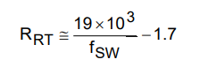
Using the above equation, we calculate the frequency setting resistor, where RRT is in kΩ and fSW is in kHz. For this design, a 61.9kΩ resistor was used for RRT to obtain approximately 300kHz switching frequency, which permits high-efficiency operation.
Step 3: Choosing the Input Capacitor
The input current of the buck regulator is inherently discontinuous. This discontinuous input current demands AC from the source and, hence, adds additional losses. A shunt input capacitor is used to filter the AC. The input capacitor is selected based on the maximum input voltage, allowable input voltage ripple, and the RMS current imposed on the capacitor. Below are the equations used for calculating the RMS current through the capacitor and required capacitance. The worst-case RMS current occurs when VIN = 2 x VOUT, which is what we assume to obtain a worst-case estimate for RMS current. The maximum duty cycle occurs when the input voltage is at a minimum. The maximum duty cycle is used to determine the input capacitance. To determine the input capacitance, we must estimate the expected efficiency. Using the MAX17506 data sheet efficiency curves, we expect a minimum 92% efficiency.
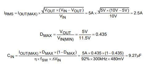
The input capacitor must be able to withstand the maximum input voltage; thus, we select a 50V rated capacitor, which is well beyond the maximum input voltage. In addition, we must ensure the RMS ripple through the capacitor does not cause any significant heating. As a rule of thumb, we limit the capacitor to a maximum 10°C rise in temperature based on the ripple current. To achieve this, we use two 4.7μF ceramic capacitors (UMK316AB7475ML) in parallel. This reduces the ripple requirement on each capacitor by half since they are in parallel (e.g., 1.25ARMS per capacitor). Based on the capacitor data sheet, each capacitor produces approximately a 3°C rise in temperature for an RMS current of 1.25A, which is within our specification.
Additionally, we place two small 0.1μF capacitors close to the IC to reduce the effects of trace impedance. These capacitors also see the full input voltage, so they must be rated for 50V
In applications where the source is located distant from the MAX17506, an electrolytic capacitor should be added in parallel to the ceramic capacitor. Doing so provides necessary damping for potential oscillations caused by the inductance of the longer input power path and input ceramic capacitor.
Step 4: Choosing the Inductor
A high-valued inductor results in reduced inductor-ripple current, leading to a reduced output-ripple voltage. However, a large inductance requires a larger physical size or higher DCR with a lower saturation current rating. The inductor is chosen based on the IC data sheet equation as follows:
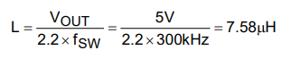
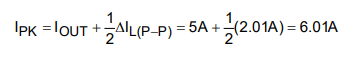
We select a 6.8μH inductance, which is approximately 10% less than the calculated value. This inductance allows for a smaller inductor and faster transient response. The next important parameter to consider is the inductor saturation current. The inductor saturation current must be higher than the peak current in the inductor. First, we calculate the ripple current in the inductor. Then, we derive the peak current based on the average current through the inductor, which is equivalent to the average load current. To calculate the peak inductor current, the following equations are used:
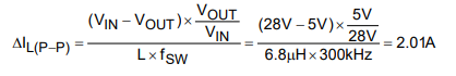
Moreover, the inductor peak current is given by:
In addition to these calculated parameters, we must also choose an inductor with low DCR and a maximum 4mm seated height. A low DCR must be selected per the IC data sheet recommendations to provide high efficiency and fast transient response. The maximum 6mm seated height results in a low-profile design for size-constrained applications, such as power supplies in modern flatscreen TVs. This design uses a 4-layer board with a 2mm thickness, so we must ensure the height of our inductor is 4mm or less.
Considering these previously derived parameters, we select the ETQP4M6R8KVC low-profile inductor with the following specifications:
| Parameter | Value |
| L | 6.8μH ±20% |
| DCR | 20.35mΩ (max) |
| ISAT | 12.1A |
| Height | 4mm |
Step 5: Choosing the Output Capacitor
The output capacitor is selected based on either a ripple voltage or a load transient requirement. This design focuses on maintaining the output voltage within 5% upon a 0A to 2.5A load transition. The IC data sheet equations for calculating the output capacitance based on a load transient are shown below:
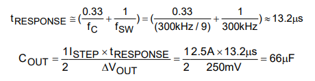
Based on the parameter used, the resulting controller response time (tRESPONSE) is 13.2μs and the output capacitance is calculated to be 66μF. The voltage rating of the capacitor must be greater than the output voltage, so we select a 10V rated ceramic capacitor. We must also allow for a ±10% capacitor tolerance and a further reduction of 20% capacitance due to the DC bias effect (i.e., operating a 10V ceramic capacitor at 5V), so our final nominal value is:
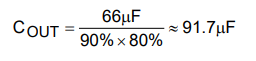
We achieve this by placing three 33μF capacitors (TDK C3216X5R1A336M160AB) in parallel.
Step 6: Choosing the Low-Side Switch
The low-side switch must be an nFET type to ensure proper operation. The switch is chosen based on the rated voltage, rated current, and on-resistance. The rated voltage is simple, since the maximum voltage the nFET sees is equivalent to the supply voltage. Thus, we must select an nFET with VDS(MAX) > VIN(MAX). The peak current in the lowside switch is equivalent to the peak current in the inductor, which was previously calculated to be 6.01A. We must select an nFET with a peak current rating above 6.01A. Finally, we select the RDS(ON) to be as low as possible.
Based on the requirements above, we select the Vishay SiS406DN with the following specifications:
| Parameter | Value |
| VDS | 30V |
| ID | 12.2A at VGS = 4.5V |
| RDS(ON) | 14.5mΩ at VGS = 4.5V |
| PMAX | 1W at TA = +70°C |
We must ensure the power dissipated in the low-side switch does not violate its maximum power dissipation. To do so, we use the following equation to determine the power dissipated in the low-side switch based on maximum load current, RDS(ON), and minimum duty cycle. The duty cycle for a buck converter is simply the ratio of the output voltage to input voltage. The minimum duty cycle occurs at maximum input voltage.
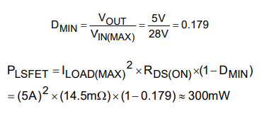
The power dissipation in the low-side switch is calculated to be approximately 300mW, which is far less than the nFET power rating. Thus, we conclude this device will work under the designed operating conditions
Last, we place a small series resistor at the nFET’s gate to limit the nFET’s slew rate. By limiting the nFET’s slew rate, we reduce the potential for switch-node ringing, voltage spikes, and EMI. A small 4.7Ω series resistor is used but can be increased if greater EMI suppression is required. However, using too large of a resistor significantly slows the transition and causes cross-conduction. Thus, it is best to start with a low value series resistor and increase resistance to achieve the desired performance.
Step 7: Setting the Output Voltage
The output voltage is determined by the voltage divider in the feedback loop, which consists of resistors R3 and R4. These resistor values are calculated using the following IC data sheet equations:
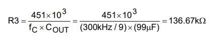
Thus, we select R3 = 137kΩ ±1%, which is connected from VOUT to FB.
Next, we calculate resistor R4, which is connected from FB to SGND:
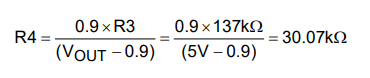
Thus, we select R4 = 30kΩ ±1%.
Step 8: Choosing the Soft-Start Capacitor
Soft-start limits the inrush current by slowly ramping up the output voltage. A longer soft-start time reduces the charging rate of the output capacitor, thereby limiting the inrush current. The required soft-start time is dependent on the output voltage and output capacitance. We must ensure the selected soft-start time does not cause any harmful inrush currents; thus, the MAX17506 data sheet provides a simple equation to ensure the soft-start time is long enough to limit the inrush current to an acceptable level.

Based on this equation, we must select CSS to be greater than 13.86nF. For this design, we select a CSS = 22nF, which produces an approximately 4ms soft-start time.
Step 9: Setting Up Bootstrap Operation
The MAX17506 internal electronics are powered by either the VCC pin or the EXTVCC pin. The VCC input uses a high-voltage LDO to regulate the input voltage to a lower system voltage, which is very inefficient when the input voltage is very large. Higher efficiencies can be achieved by using the buck output as input to a lower voltage LDO. To take advantage of this unique feature, we simply connect the buck output to the EXTVCC pin. An RC filter is added between the buck output and the EXTVCC input to increase PSRR.
We begin by selecting the filter’s series resistance. The minimum operating voltage of the low-voltage LDO is 4.84V minimum; thus, we must ensure that the voltage drop across the series resistor does not cause an undervoltage condition. To ensure this does not occur, we assume a worst-case 2mA operating current. This 2mA of operating current should not cause more than 10mV drop across the series resistor. The following equation is used to estimate the size of the series resistor:

Thus, we select RS = 4.7Ω.
Finally, we select the filter capacitor to achieve a 3dB attenuation of the fundamental switching frequency. A 3dB attenuation occurs at the RC filters pole; therefore, we use the following equation to select the shunt filter capacitor:
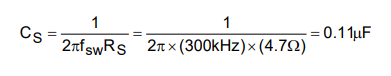
Thus, we select CS = 0.1μF.
Step 10: Setting the UVLO
UVLO turns the converter off when the input voltage is below a set threshold. The following equations are used to find the resistor-divider values that produce an 11.5V input threshold.
R1 = 3.3MΩ, per the data sheet recommendations.
Thus, we select R1 = 3.32MΩ ±1% standard value resistor.
The input voltage threshold is reduced by 2% to account for resistor tolerances. This ensures the UVLO only asserts below 11.5V.

Thus, we select R2 = 402kΩ ±1% standard value resistor.
Step 11: Choosing the BST Capacitor
An external flying capacitor is used by the MAX17506’s internal electronics. This flying capacitor provides power for the internal high-side driver circuitry. Connect a 0.1μF capacitor between BST and LX. A ceramic capacitor with a 16V rating or greater is recommended.
Step 12: Choosing the Compensation Capacitor
The MAX17506 is internally compensated; however, since the switching frequency is less than 450kHz, we must connect a 2.2pF capacitor between the CF pin and the FB pin. CF and FB are low-voltage pins used by the internal control loop; thus, we select a 10V rated ceramic capacitor.
関連資料
-
MAXREFDES1034 Design Files2019/07/09ZIP9 M
-
EE-Sim OASIS Free Simulator2019/07/09
-
MAXREFDES1034: High-Efficiency Power Supply for TVs Using MAX175062019/07/09PDF439K
サポートおよびトレーニング
技術的なご質問についての回答は、ナレッジベースを検索してください。また、アナログ・デバイセズのアプリケーション・エンジニアの専任チームが、技術的なご質問にお答えいたします。