


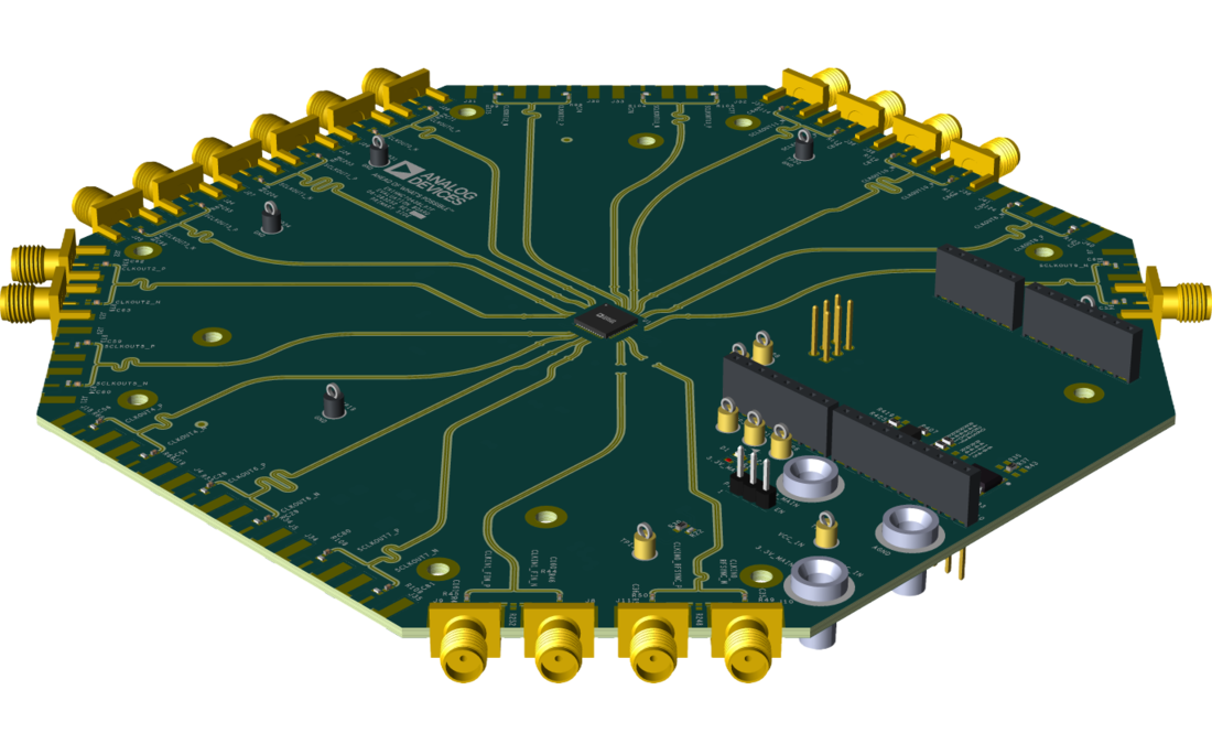
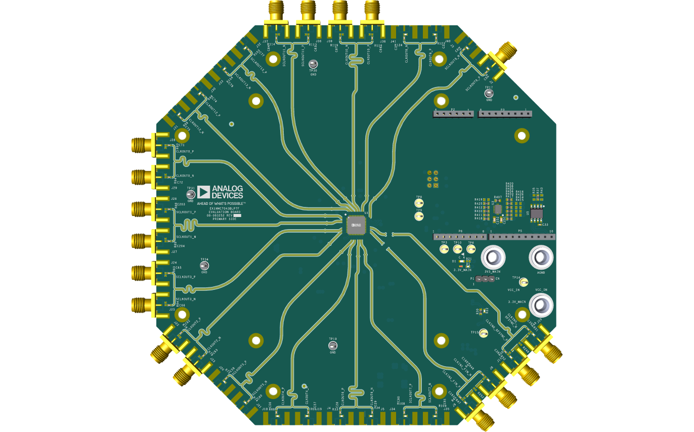
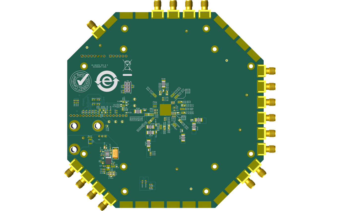
製品概要
機能と利点
- HMC7043B(高性能な3.2GHzの14出力ファンアウト・バッファ)、SDP-K1 Arduinoインターフェース、電圧レギュレータを搭載した自己完結型ボード
- クロック入力1系統、RFSYNC入力1系統、クロック出力6系統用のSMAコネクタ
- Windows®ベースのソフトウェアにより、PCから制御可能
- 6V~14Vの外部電源
製品概要
このユーザ・ガイドでは、HMC7043B評価用キットのハードウェアとソフトウェアについて説明します。本評価用ボードの回路図とプリント回路基板(PCB)のレイアウト・アートワークについては、EK1HMC7043BLP7Fの製品ページ(www.analog.com/jp)を参照してください。
HMC7043Bは、パラレルまたはシリアル(JESD204Bタイプ)インターフェースを備えた高速データ・コンバータ向けに、超低位相ノイズのリファレンスを分配する高性能クロック・バッファです。HMC7043Bは、マルチキャリアGSMおよびLTE基地局設計の要件を満たすように設計されており、広範なクロック管理と分配機能を提供し、ベース・バンドと無線カードのクロック・ツリーの設計を簡素化します。
EK1HMC7043BLP7F評価用キットは、HMC7043Bの全機能を評価できる、コンパクトで使いやすいプラットフォームです。EK1HMC7043BLP7F評価用ボードでは、すべての入力と出力は差動として設定されます。
HMC7043Bの詳細な仕様は、この製品のデータシートに記載されています。本評価用ボードを使用する際は、このユーザ・ガイドと併せてHMC7043Bのデータシートも参照してください。
対象となる製品
はじめに
必要な装置
- USBポートを備えたWindowsベースのPC(評価用ソフトウェアを実行)
- システム・デモンストレーション・プラットフォームEVAL-SDP-CK1Z(SDP-K1)
- 電源(6V~14V)
- 50Ωの終端
- 低ノイズの外部CLKININソース
関連資料
-
UG-2359: Evaluating the HMC7043B 14 Outputs Jitter Attenuator (Rev. 0)2026/08/19PDF6 MB