DS26303ショートホールラインインタフェースユニットとIDT82V2048
要約
この文書では、既存のIDT82V2048アプリケーションでDS26303を使うために必要となる情報に重点をおきつつ、DS26303とIDT82V2048の違いについて説明します。機能の違い、レジスタについて、およびハードウェアについての説明を提供します。
はじめに
この文書では、既存のIDT82V2048アプリケーションでDS26303を使うために必要となる情報に重点をおきつつ、DS26303とIDT82V2048の違いについて説明します。DS26303は、3.3V単一電源で動作してE1/T1/J1をサポートする、8チャネルのショートホールラインインタフェースユニット(LIU)です。このデバイスは、ソフトウェアの変更なしでIDT82V2048の機能をサポートするとともに、さらに追加の機能を提供します。DS26303は、PCBレイアウトを変更することなく、希望のアプリケーションに合わせて単に外付け部品の値を変えるだけで、既存のIDT82V2048アプリケーションで使用することができます。
機能の違いは、3つのセクションに分けて説明します。表1では、DS26303の機能の中でIDT82V2048には存在しないものの一覧を示します。表2では、IDT82V2048の機能の中でDS26303には存在しないものの一覧を示します。表3では、DS26303とIDT82V2048の両方に存在しており、かつ両方のデバイスで同じ実装になっていない機能の一覧を示します。
DS26303とIDT82V2048のレジスタの違いについては、DS26303で追加されたレジスタバンクによって提供される追加機能と合わせて、表6~表10で説明します。図1と表11では、DS26303を既存のIDT82V2048アプリケーションで使用する場合に必要となる、部品の値の細かな変更について示します。
| DS26303 | IDT82V2048 |
| Programmable option to clear interrupt status on write or read. Clear on read is default. | Not supported. |
| Individual channel control for jitter attenuator:
|
All channels have global control. |
| Internal software-selectable transmit and receive-side termination for 100Ω T1 twisted-pair, 110Ω J1 twisted-pair, 120Ω E1 twisted-pair, and 75Ω E1 coaxial applications. | Not supported. |
| In HPS mode, the transmitter output and the internal impedance of the receiver can be turned off with only the OE pin. | Requires that both receivers use the same front-end termination. |
| Built in BERT tester for diagnostics. | Not supported. |
| Individual channel control for:
|
All channels have global control. |
| Individual channel-line violation detection. | Not supported. |
| Flexible MCLK See Table 4 for available input frequencies. | Not supported. |
| Programmable TECLK output pin (1.544MHz or 2.048MHz) | Not supported. |
| Programmable CLKA output pin See Table 5 for available output frequencies. | Not supported. |
| Flexible interrupt pin | Not supported. |
| DS26303 | IDT82V2048 |
| Uses single optimal value. | Capability to select the jitter attenuator bandwidth. |
| Not provided. | Inband loopack (loopup and loopdown codes). |
| MLCK Pin Functionality The DS26303 and IDT82V2048 both require MCLK to for data with clock recovery as well as AIS detection. The MCLK pin of the IDT82V2048 provides additional functionality not present in the DS26303. IDT82V2048 MCLK held high. IDT82V2048 MCLK held low. Note that wait state generation through RDY/ACK is not available if MCLK is not provided. |
|
| DS26303 | IDT82V2048 |
| 3.3V LIU power only, 5V not provided. | 5V LIU power. |
| Non-mux Intel® write address to WRB rising-edge setup time is 17ns. | Non-mux Intel write address to WRB rising-edge setup time is 6ns. |
| Expects non-mux Intel read address to be valid when RDB is active. | Non-mux Intel read address to RDB rising-edge setup time is 6ns. This might be an error in data sheet because data is out before this setup time. |
| Inactive RDY to tri-state delay time 12ns (max). | Inactive RDY to tri-state delay time 3ns (max). |
| Clears the interrupt pin when reading or writing the interrupt status. | Clear interrupt pin by reading the corresponding status register. |
| Jitter attenuator FIFO depths of 32 bits or 128 bits. | Jitter attenuator FIFO depths of 32 bits or 64 bits. |
| Individual channel control for jitter attenuator: |
All channels have global control. |
| PLLE | MPS1, MPS0 | MCLK MHz (±50ppm) | FREQS | T1 or E1 Mode |
| 0 | xx | 1.544 | x | T1 |
| 0 | xx | 2.048 | x | E1 |
| 1 | 00 | 1.544 | 1 | T1/J1 or E1 |
| 1 | 01 | 3.088 | 1 | T1/J1 or E1 |
| 1 | 10 | 6.176 | 1 | T1/J1 or E1 |
| 1 | 11 | 12.352 | 1 | T1/J1 or E1 |
| 1 | 00 | 2.048 | 0 | T1/J1 or E1 |
| 1 | 01 | 4.096 | 0 | T1/J1 or E1 |
| 1 | 10 | 8.192 | 0 | T1/J1 or E1 |
| 1 | 11 | 16.384 | 0 | T1/J1 or E1 |
| CLKA3 to CLKA0 | MCLK (Hz) |
| 0000 | 2.048M |
| 0001 | 4.096M |
| 0010 | 8.192M |
| 0011 | 16.384M |
| 0100 | 1.544M |
| 0101 | 3.088M |
| 0110 | 6.176M |
| 0111 | 12.352M |
| 1000 | 1.536M |
| 1001 | 3.072M |
| 1010 | 6.144M |
| 1011 | 12.288M |
| 1100 | 32k |
| 1101 | 64k |
| 1110 | 128k |
| 1111 | 256k |
レジスタについて
DS26303には、4つの主なレジスタバンクが含まれています。
- プライマリレジスタ(DS26303およびIDT82V2048)
- セカンダリレジスタ(DS26303およびIDT82V2048)
- I個別LIUレジスタ(DS26303のみ)
- BERTレジスタ(DS26303のみ)
DS26303の追加機能と柔軟性を利用するためには、IDT82V2048アプリケーション向けに書かれたすべてのオリジナルソースコードに、新規コードを追加する必要があります。アドレスポインタ制御レジスタ(ADDP、アドレス1Fh)が、希望のレジスタバンクにアクセスするためのポインタとして使用されます。表6に、DS26303のレジスタバンクの一覧と、希望のレジスタバンクにアクセスするために必要となるADDPの値を示します。
| ADDP7 to ADDP0 (Hex) | Bank Name | DS26303 | IDT82V2048 |
| 00 | Primary Bank | Yes | Yes |
| AA | Secondary Bank | Yes | Yes |
| 01 | Individual LIU Bank | Yes | No |
| 02 | BERT Bank | Yes | No |
DS26303のプライマリレジスタバンクは、IDT82V2048のものと同じです。DS26303を既存のIDT82V2048の代わりに使用し、かつプライマリレジスタバンクだけを使用する場合は、アプリケーションソフトウェアの変更は必要ありません。表7に、プライマリレジスタの概要を示します。
| Address (Hex) | DS26303 and IDT82V2048 |
| 00–15 | Primary Registers |
| 16–1E | Reserved |
| 1F | ADDP |
DS26303とIDT82V2048は、どちらもセカンダリレジスタバンクを提供していますが、すべてのレジスタの名称や機能が同じわけではありません。表8に、DS26303とIDT82V2048のセカンダリレジスタバンクに含まれるレジスタの一覧およびそれらの機能を示します。
DS26303には、他にさらに2つのレジスタバンクが含まれています。個別LIUレジスタバンクとBERTレジスタバンクです。個別LIUレジスタバンクに含まれるレジスタの一覧を表9に、BERTレジスタバンクに含まれるレジスタの一覧を表10に、それぞれ示します。DS26303の追加機能と柔軟性を利用するためには、IDT82V2048アプリケーション向けに書かれたすべてのオリジナルソースコードに、新規コードを追加する必要があります。
| Address (Hex) | Register Name | DS26303 | IDT82V2048 |
| 00 | Single-Rail Mode Select | Yes | Yes |
| 01 | Line-Code Selection | Yes | Yes |
| 02 | Clock-Recovery Enable | No | Yes |
| 03 | Receiver Power-Down Enable | Yes | Yes |
| 04 | Transmitter Power-Down Enable | Yes | Yes |
| 05 | Excessive Zero-Detect Enable | Yes | Yes |
| 06 | Code-Violation-Detect Enable Bar | Yes | Yes |
| 07 | Receive Equalizer Enable | No | Yes |
| 08 | Inband Loopback (LB) Configuration | No | Yes |
| 09 | Inband LB Activation Code | No | Yes |
| 0A | Inband LB Deactivation Code | No | Yes |
| 0B | Inband LB Receive Status | No | Yes |
| 0C | Inband LB Interrupt Mask | No | Yes |
| 0D | Inband LB Interrupt Status | No | Yes |
| 0E | Inband LB Activation/Deactivation Code Generator | No | Yes |
| 1F | Set to AAh for access to Secondary Register Bank | Yes | Yes |
| Address (Hex) | Register Name |
| 00 | Individual JA Enable |
| 01 | Individual JA Position Select |
| 02 | Individual JA FIFO Depth Select |
| 03 | Individual JA FIFO Limit Trip |
| 04 | Individual Short-Circuit Protection Disable |
| 05 | Individual AIS Select |
| 06 | Master-Clock Select |
| 07 | Global-Management Register |
| 08–0F | Reserved |
| 10 | Bit-Error-Rate Tester Control Register |
| 12 | Line-Violation Detect Status |
| 13 | Receive-Clock Invert |
| 14 | Transmit-Clock Invert |
| 15 | Clock-Control Register |
| 16 | RCLK Disable Upon LOS Register |
| 1E | Global-Interrupt Status Control |
| 1F | Set to 01h for access to Individual LIU Register Bank |
| Address (Hex) | Register Name |
| 00 | BERT Control Register |
| 01 | Reserved |
| 02 | BERT Pattern Configuration 1 |
| 03 | BERT Pattern Configuration 2 |
| 04 | BERT Seed/Pattern 1 |
| 05 | BERT Seed/Pattern 2 |
| 06 | BERT Seed/Pattern 3 |
| 07 | BERT Seed/Pattern 4 |
| 08 | Transmit-Error Insertion Control |
| 09–0A | Reserved |
| 0C | BERT Status Register |
| 0D | Reserved |
| 0E | BERT Status Register Latched |
| 10 | BERT Status Register Interrupt Enable |
| 11–13 | Reserved |
| 14 | Receive Bit-Error Count Register 1 |
| 15 | Receive Bit-Error Count Register 2 |
| 16 | Receive Bit-Error Count Register 3 |
| 17 | Receive Bit-Error Count Register 4 |
| 18 | Receive Bit-Count Register 1 |
| 19 | Receive Bit-Count Register 2 |
| 1A | Receive Bit-Count Register 3 |
| 1B | Receive Bit-Count Register 4 |
| 1C–1E | Reserved |
| 1F | Set to 02h for access to BERT Register Bank |
ハードウェアについて
DS26303は、PCBレイアウトを変更することなく、既存アプリケーション内のIDT82V2048の代わりに使用することができます。必要なのは、希望するアプリケーションに応じて、外付け部品の値を変更することだけです。推奨されるDS26303のネットワーク終端回路を図1に、またDS26303を適切に終端させるための各部品の値を表11に示します。
トランスミッタ
IDT82V2048は、TTIPおよびTRING出力と直列に送信側抵抗を必要とします。IDT82V2048ではこれらの抵抗は、0Ω (T1 3.3Vモード)、9.5Ω (E1 75Ω同軸)、または9.1Ω (E1 120Ωツイストペア)が推奨されています。DS26303は抵抗を必要としないため、存在する場合はすべてのモードにおいて0Ωにしてください。
レシーバ
受信側では、IDT82V2048は12.4Ω (T1 3.3Vモード)、9.31Ω (E1 75Ω同軸)、または15Ω (E1 120Ωツイストペア)の終端抵抗を必要とします。DS26303、外部インピーダンスモードを使用している場合、すべてのモードについて15Ωの終端抵抗を必要とします。ソフトウェアで選択可能なDS26303のインピーダンス整合モードを使用している場合は、これらの抵抗は必要ありません。IDT82V2048はRTIPおよびRRING端子と直列に1kΩの抵抗を必要とします。ソフトウェア終端/インピーダンス整合を希望する場合は、これらの1kΩ抵抗を0Ω抵抗に取り替えてください。
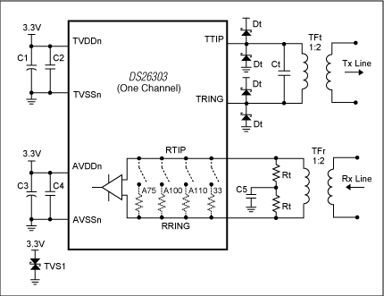
図1. LIUフロントエンド。
| Mode | Component | 75Ω Coaxial | 120Ω Twisted Pair | 100Ω/110Ω Twisted Pair |
| Tx Capacitance | Ct | 560pF (typ). Adjust for board parasitics for optimal return loss. | ||
| Tx Protection | Dt | International Rectifier: 11DQ04 or 10BQ060 Motorola: MBR0540T1 | ||
| Rx Transformer 1:2 | TFr | Pulse: T1124 (0°C to +70°C) | ||
| Tx Transformer 1:2 | TFt | Pulse: T1114 (-40°C to +85°C) | ||
| Tx Decoupling (ATVDD) | C1 | Common decoupling for all eight channels is 68µF. | ||
| Tx Decoupling (ATVDD) | C2 | Recommended decoupling per channel is 0.1µF. | ||
| Rx Decoupling (AVDDn) | C3 | Common decoupling for all eight channels is 68µF. | ||
| Rx Decoupling (AVDDn) | C4 | Common decoupling for all eight channels is 0.1µF. | ||
| Rx Termination | C5 | When in external impedance mode, Rx capacitance for all eight channels is 0.1µF. Do not populate if using internal impedance mode. | ||
| Rx Termination | Rt | When in external impedance mode, the two resistors for all modes shall be 15.0Ω ±1%. Do not populate if using internal impedance mode. | ||
| Voltage Protection | TVS1 | SGS-Thomson: SMLVT 3V3 (3.3V transient suppressor) | ||
DS26303に関するその他の情報
マキシムの通信製品の詳細については、データシートを参照してください。 これらの通信デバイスの操作に関してさらに質問がある場合は、アナログ技術サポート チームにお問い合わせください。