Design Note 240: ADSL Modems That Use the LT1886 As a Line Driver Yield Long Reach and Fast Data Rates
ADSL technology allows for communication to a remote internet server at data rates nearing 1Mbit/sec, nearly twenty times faster than conventional modems, over normal telephone wiring with a reach of up to 18,000 feet. A key component in making this happen is the power amplifier used to drive the encoded data signal on to the phone line. Ideally the line driver must not introduce any distortion of the transmitted signal. This allows the system to maximize the data rate over the longest wiring reach possible by using all of the available carrier tones for the data transmission. The LT1886 line driver outputs undistorted broadband power into the telephone network.
The LT1886 also maintains very low distortion even when configured for high levels of closed-loop gain. Low supply voltage VLSI digital circuits used to provide the encoded data require significant voltage gain to be taken in the line driver without introducing distortion.
LT1886: Low Distortion Line Driver
The LT1886 is a high speed dual power amplifier with excellent high frequency distortion performance. The LT1886 features a 700MHz gain-bandwidth product, 200V/μs slew rate and over 200mA of output current drive in a small SO-8 package. Using only a single 12V supply, the LT1886 is the best choice for the line driver in ADSL CPE modems (customer premises equipment).
Figure 1 illustrates a differential line driver with an LT1886 driving a 1:2 turns ratio isolation/coupling transformer. Here it can be seen that both the 2nd and 3rd harmonic components of a 200kHz tone, even with a closed-loop gain of 10, are well below –80dBc with nominal signal power of 13dBm, 4VP-P placed on the line. The distortion remains less than –70dBc during large-signal transients, 15VP-P, which occur often in the complex modulated ADSL transmission signal. The nominal RMS output current from the driver during an ADSL transmission is only 30mA, but the peak driver current capability must be greater than 160mA. To prevent distorting the signal, the line driver cannot current limit.

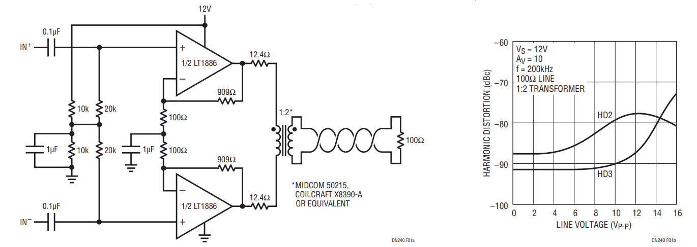
Figure 1. A Single 12V Supply ADSL Modem Line Driver with Low Harmonic Distortion Performance.
Traditionally, the power stage is the limiting factor for high frequency performance. The LT1886 is fabricated with an advanced low voltage complimentary bipolar process that combines high frequency amplification with output power handling capability. In addition, to obtain the best distortion performance possible, an amplifier must sustain a very high open-loop gain to as high of a frequency as is practical.
LT1886 Frequency Response
Figure 2 illustrates the gain and phase shift response versus frequency of the LT1886. The amplifier is a voltage feedback design which is compensated for gains greater than 10 and has a conventional single pole open-loop gain roll off characteristic.

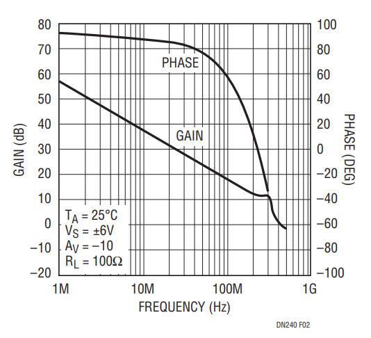
Figure 2. Open-Loop Gain and Phase vs Frequency.
The low frequency open-loop gain is over 80dB out to a frequency of 60kHz, a gain-bandwidth product of approximately 700MHz. Notice that with a closed-loop gain of 10 (20dB), the closed-loop bandwidth is 70MHz and the phase margin is nearly 70°, resulting in very stable operation. However, the amplifier is intentionally decompensated to maximize gain bandwidth for distortion performance. At the frequency where the phase margin drops to 0°, approximately 230MHz, the amplifier still has 12dB of gain. With a closed-loop gain this low the amplifier will oscillate.
For stability, it is important for the amplifier to always have a feedback factor of 0.1 or less to maintain a noise gain value of 10 or more. For this reason, in Figure 1, the two 100Ω gain setting resistors for the driver are returned to a good AC ground provided by the 1μF bypass capacitor. This ensures that the impedance from the inverting inputs to ground, even beyond 300MHz where the LT1886 still has gain, is controlled and held at a low enough value for stable operation.
A Circuit “Trick” for a Gain of Less Than 10
In many applications, it may still be desired to operate the driver stage with a gain of less than 10. In this case, a simple circuit “trick” for decompensated op amps can be employed. The addition of a resistor (and an optional capacitor) between the two inputs of the amplifier can provide stable operation at any desired closed-loop gain. Figure 3 illustrates these gain compensation components for inverting and noninverting amplifiers.

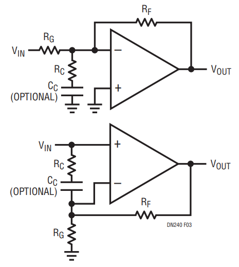
At lower frequencies, where the open-loop gain of the amplifier is very high, there is very little signal between the two inputs. With no signal across the compensating resistor, RC, it is effectively out of the circuit. The feedback resistor, RF, and the gain setting resistor, RG, then determine the closed-loop gain of the amplifier. At higher frequencies, as the open-loop gain reduces, a signal is developed across RC and it becomes part of the circuit and effectively parallels resistor RG. This assumes that the impedance to ground at the noninverting input is much lower than the feedback component values. The lower value of RG reduces the feedback factor and in essence tricks the amplifier into operating at a higher gain. The following equation can be used to determine the value for RC to ensure stability with lower than required closed-loop gain:
RC = RF / AVREQUIRED – AVACTUAL
Where AVREQUIRED is 10 and AVACTUAL is any gain between 1 and 10. Using this technique the amplifier operates with a stable lower closed-loop gain but has the bandwidth of a gain of 10 amplifier.
The capacitor, CC, is optional to prevent increased gain to the DC offset of the amplifier. For the LT1886, this capacitor should be sized together with RC to come into effect at a frequency between 5MHz and 15MHz.
著者
